<< Chapter < Page Chapter >> Page >
This last part of the main text of IC journey from 1959 to 2009 gives cost metrics of IC Chip. It gives the algorithm to determine the cost of a die.

Reference materials:ECE4121/ECE4141,VLSI Design,Design Metrics by AHM Zahirul Alam.

Cost of IC Chip=Non-recurring expenditure(NRE)+Recurring Expenditure(RE)

NRE is the fixed cost of mask generation. It is one-time cost factor.

RE is the expenditure incurred in Silicon procesing, packaging, volume of production and the die area.

70nm ASIC incurs $4M NRE on account of masks.

"The club of people who can offer an extreme sub-micron ASIC or COD design is getting pretty exclusive."Ron Wilson,EE Times (May,2000)

The Cost Metrics of the IC Chip.

Chip M.L L.W(μm) W.C($) W.D(mm) D/cm 2 D.S.(mm) D(mm 2 ) D/W Y(%) D.C.($)
386DX 2 0.9 900 150 1 10 43 360 71 4
486DX2 3 0.8 1200 150 1 12 81 181 54 12
P.PC601 4 0.8 1700 150 1.3 121 115 28 53
_7100 3 0.8 1300 150 1 196 66 27 73
DECα 3 0.7 1500 150 1.2 234 53 19 149
S.SPARC 3 0.7 1700 150 1.6 256 48 13 272
Pent. 3 0.8 1500 150 1.5 18 296 40 9 417

M.L.-metal layers, L.W.-line width,W.C.-Wafer Cost,W.D.-Wafer Diameter(mm),D./cm^2-defects per cm square,D.S.-die size(mm),D(mm^2)-Die Area(mm square),D/W-Dies/Wafer, Y-Yield,D.C.-Die Cost($)

Algorithm for calculating the die cost:

Recurring costs:

Variable Cost =

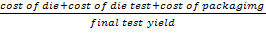
Where : Cost of Die =

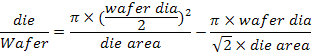
die yield= [1+((defect/area)*(die area))/alpha]^(-alpha)

One example:

Wafer size = 12’’ = 30.48 cm;

Die size = 2.5 cm 2 ;

1 defect/cm 2 ;

alpha=α= 3( complexity);

Number of dies per wafer = 252 dies /wafer;

Die yield = 16 %;

252×0.16 = 40 die/wafer;

40 die per wafer can actually be marketed.

Hence die cost = wafer cost/40 ;

Die cost is a strong function of die area.

Die cost is proportional to the Nth power of die area where n=3 to 4.

Questions & Answers

what is phylogeny
Odigie Reply
evolutionary history and relationship of an organism or group of organisms
AI-Robot
ok
Deng
what is biology
Hajah Reply
the study of living organisms and their interactions with one another and their environments
AI-Robot
what is biology
Victoria Reply
HOW CAN MAN ORGAN FUNCTION
Alfred Reply
the diagram of the digestive system
Assiatu Reply
allimentary cannel
Ogenrwot
How does twins formed
William Reply
They formed in two ways first when one sperm and one egg are splited by mitosis or two sperm and two eggs join together
Oluwatobi
what is genetics
Josephine Reply
Genetics is the study of heredity
Misack
how does twins formed?
Misack
What is manual
Hassan Reply
discuss biological phenomenon and provide pieces of evidence to show that it was responsible for the formation of eukaryotic organelles
Joseph Reply
what is biology
Yousuf Reply
the study of living organisms and their interactions with one another and their environment.
Wine
discuss the biological phenomenon and provide pieces of evidence to show that it was responsible for the formation of eukaryotic organelles in an essay form
Joseph Reply
what is the blood cells
Shaker Reply
list any five characteristics of the blood cells
Shaker
lack electricity and its more savely than electronic microscope because its naturally by using of light
Abdullahi Reply
advantage of electronic microscope is easily and clearly while disadvantage is dangerous because its electronic. advantage of light microscope is savely and naturally by sun while disadvantage is not easily,means its not sharp and not clear
Abdullahi
cell theory state that every organisms composed of one or more cell,cell is the basic unit of life
Abdullahi
is like gone fail us
DENG
cells is the basic structure and functions of all living things
Ramadan
What is classification
ISCONT Reply
is organisms that are similar into groups called tara
Yamosa
in what situation (s) would be the use of a scanning electron microscope be ideal and why?
Kenna Reply
A scanning electron microscope (SEM) is ideal for situations requiring high-resolution imaging of surfaces. It is commonly used in materials science, biology, and geology to examine the topography and composition of samples at a nanoscale level. SEM is particularly useful for studying fine details,
Hilary
Got questions? Join the online conversation and get instant answers!
Jobilize.com Reply

Get Jobilize Job Search Mobile App in your pocket Now!

Get it on Google Play Download on the App Store Now


Source:  OpenStax, Solid state physics and devices-the harbinger of third wave of civilization. OpenStax CNX. Sep 15, 2014 Download for free at http://legacy.cnx.org/content/col11170/1.89
Google Play and the Google Play logo are trademarks of Google Inc.

Notification Switch

Would you like to follow the 'Solid state physics and devices-the harbinger of third wave of civilization' conversation and receive update notifications?

Ask