

| << Chapter < Page | Chapter >> Page > |
Thermal and Thermofluid modeling software is being accepted for simulation based development and implementation of advanced packages. High performance, air-cooled heat sinks will dominate future applications.
7.7.11.The Challenges being posed by Scaling.
7.7.11.1. High-K dielectric for Gate Insulation.
The biggest challenge is the unacceptably thin gate oxide with advanced scaling.
Table 7.7.11.1 gives the thicknesses of gate oxide with advanced Generation of MOS devices.
Table 7.7.11.1. The Gate Oxide Thickness (D nm) in advanced Generations of Devices.
| Generation | 5μm | 2μm | 1.2μm | 90nm | 45nm | 30nm |
| D(nm) | 88nm | 40nm | 22nm | 1.3nm | ? | ? |
We see that as we reach 90nm Generattion of Devices, the oxide layer becomes:
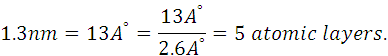
At 5 atomic layer thick Gate Oxide direct Quantum Mechanical tunneling is enabled leading to high Gate leakage and increased static power dissipation. The only solution was to make it physically thick but keep it electrically thin so that threshold voltage is unaffected., So we go for high K dielectric material for gate insulation.
Since Gate Capacitance has to remain constant therefore:
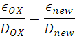
Therefore:
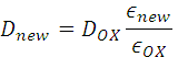
So if a high K material 5× the dielectric constant of SiO 2 is used we will have 5× thick oxide layer that is 6.5nm thick dielectric material at the Gate which will completely cutoff the leakage and hence we normalize the statric power dissipation to nW in CMOS logic..
High K dielectrics are HfO 2 with K=15 to 30 or HfSiO 2 with K= 12 to 16..
7.7.11.2. Poly-Silicon Gate should be replaced by Metal as Silicon Dioxide replaced by High-K insulator.
The scaling forces SiO 2 to be replaced by high-K insulator but it simultaneously demands Poly-Si to be replaced by Metal. As we progress with scaling Poly-Si becomes less effective as Gate. There are three reasons for this:
Therefore Poly-Si has to be replaced by Metal again as it was in the start of IC
Technology.
7.7.11.3.Strained Silicon for enhanced channel mobility.
To further solve the problem of reduced channel mobility, Uniaxial Process induced Stress could be used for enhanced mobility and hence for higher channel conductivity.
7.7.12. Concluding Remarks on Scaling.
Table 7.7.12.1. gives the typical scaling factors which have been used for the advanced Generations of the Devices.(Reference:”Device Scaling:The Treadmill that fuelled Semiconductor Industry Growth” by Pallab Chatterjee, i2 Technologies, Inc.)
Table. 7.7.12.1.Semiconductor Association Association 1992 Overall Road Map Technology Characteristics.
| 1992 | 1995 | 1998 | 2001 | 2004 | 2007 | |
| Node(2λ) nm | 500 | 350 | 250 | 180 | 120 | 100 |
| Scaling factor(α) | - | 1.43 | 2 | 2.8 | 4.16 | 5 |
| Desktop,V DD (V) | 5 | 3.3 | 2.2 | 2.2 | 1.5 | 1.5 |
| Portable,V DD (V) | 3.3 | 2.2 | 2.2 | 1.5 | 1.5 | 1.5 |
| Desktop, (β) | - | 1.515 | 2.27 | 2.27 | 3.33 | 3.33 |
| Portable, (β) | - | 1.5 | 1.5 | 2.2 | 2.2 | 2.2 |
| High Per.-P D (W per die) | 10 | 15 | 30 | 40 | 40-120 | 40-200 |
| Portable.-P D (W per die) | 3 | 4 | 4 | 4 | 4 | 4 |
| Clock(MHz)-off chip | 60 | 100 | 175 | 250 | 350 | 500 |
| Clock(MHz)-on chip | 120 | 200 | 350 | 500 | 700 | 1000 |
| f 0 is scaled by α 2 /β-offchip | 60 | 81 | 105 | 207 | 312 | 450 |
| f 0 according to SIA | 60 | 100 | 175 | 250 | 350 | 500 |
| f 0 is scaled by α 2 /β-on-chip | 120 | 162 | 211 | 414 | 623 | 901 |
| f 0 according to SIA | 120 | 200 | 350 | 500 | 700 | 1000 |
| Power per die(W) | 10 | 15 | 30 | 40 | 80 | 120 |
| No. of Gates per die(SIA) | 300k | 500k | 2M | 5M | 10M | 20M |
| P g (power per gate)×10 -5 W | 3.33 | 3 | 1.5 | 0.8 | 0.8 | 0.6 |
In addition to speed and packing density, scaled CMOS provides new opportunities in low power management. Speed can be traded off fiir reduction in power consumption.
40N. AA NiMH Battery Cells are required for FULL MOTION VIDEO PLAYER in 0.5μm technology.
1No. AA NiMH Battery Cells are required for FULL MOTION VIDEO PLAYER in 0.1μm technology.
This gives the kind of accessibility which can be developed for the electreonic goods with Scaling.
Notification Switch
Would you like to follow the 'Solid state physics and devices-the harbinger of third wave of civilization' conversation and receive update notifications?

|
|

|
|

|
|

|
|

|
|

|
|

|
|

|
|

|
|
|
|