

| << Chapter < Page | Chapter >> Page > |
A hybrid circuit is essentially the marriage of monolithic technology and thin film technology realizing the best of both the technologies. Thin film technology and thick film technology offer greater design freedom with respect to physical realization of passive components, resistors and capacitors, in the sense that greater range of component values, closer tolerances and lower temperature coefficients can be achieved.
There are two variations of this hybrid technology. In one variation thin film or thick film passive components are realized on a suitable substrate (such as coming glass or ceramic) and these are interconnected among themselves and to the discrete active components (diodes and transistors) situated on the same substrate by metalized interconnecting patterns. Thus the complete working circuit is achieved on the same substrate. This is strictly known as hybrid circuit.
In another variation, the active components are formed within a silicon chip and the passive components pattern is deposited by thin film techniques on top of the silicon dioxide passivating layer covering the active circuit. These are known as compatible circuits which is an extension of monolithic art.
In this Chapter we will concentrate on the state of art of Monolithic Technology.
Section (6.3) Planar Fabrication Processes for Integrated Circuits
In I.C. technology all the fabrication steps are performed at the surface of a silicon crystal and all contacts lie in one plane hence these processes are called Planar Fabrication Processes. Planar fabrication process consists of three routes for achieving monolithic circuits:
(a) The epitaxial diffusion process,
(b) The diffused-collector process, and
(c) The triple diffusion process.
Here we will describe epitaxial diffusion process which has become the standard method for fabricating IC Chips.
6.3.1 Epitaxial Diffusion Process:
Epitaxial diffusion process consists of the following steps,
(a) preparation of single crystal silicon wafer,
(b) growth of epitaxial film over the silicon wafer,
(c) growth of silicon dioxide film,
(d) photo masking and photo etching ,
(e) impurity diffusion/ion implantation,
(f) vacuum evaporation of Aluminum.
Some of the above steps are employed more than once in the sequence.
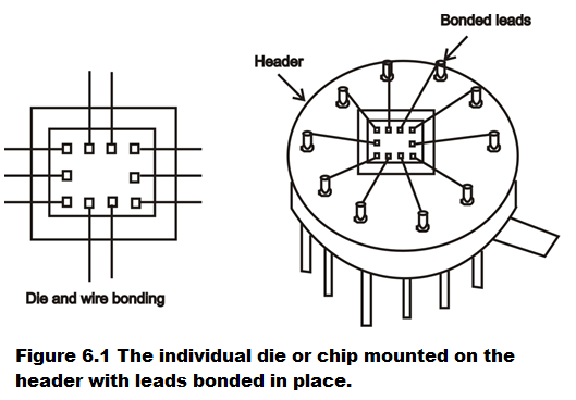
6.3.2 Mounting on header and packaging.
After these steps the wafer is scribed with a diamond-tipped scribing tool and separated into individual chips or dies. These individual silicon chips or dies are mounted on ceramic wafers by means of solder glass .The ceramic wafers are attached to suitable header by means of a high temperature eutectic solder . Or the die can be mounted in all ceramic flat package . Gold Wires only 0.001 inch in diameter are bonded from the circuit to the proper package leads by thermo-compression or ultrasonic bonding.
The header is hermetically sealed by a suitable packaging material which is impervious to moisture and gas. The packaging should satisfy the following requirements :
Notification Switch
Would you like to follow the 'Solid state physics and devices-the harbinger of third wave of civilization' conversation and receive update notifications?

|
|

|
|

|
|

|
|

|
|

|
|
|
|
|
|
|
|

|
|
|
|