

| << Chapter < Page | Chapter >> Page > |
2.2.7.1. Mobility of electron in Semiconductor is intimately connected with the structure of the Semi-conductor.
In Chapter 12, Part 12, it hasa been shown that:
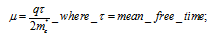
Here mean free time is a critical parameter which depends on three factors related to the structure of the Semi-conductor.:
If there were no disturbances(either due to thermal vibrations or due to defects in the crystalline structure or due to interstitial or substitutional impurities) in the orderly arrangement of the lattice centers then a mobile carrier under the application of an electric field would move in a straight line and would continue to move in straight line indefinitely even after the Electric Field is removed. This would be a living embodiment of the First Law of Newton:
A body at rest would continue to be at rest and a body in motion would continue to move in a straight line with a constant velocity unless or until made to act otherwise by the application of a force.
Such an ideal crystal would behave like a Super-conductor and its mean free time would be very large and its mobility would also be very large. .
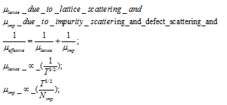
In real life we always face disorderliness due to thermal vibrations, due to lattice defect and due to impurities. This leads to scattering and this lead to finite mobility and finite resistance. Hence we have two kinds of scattering and two kinds of mobilities:
Using this theoretical formulation and experimentally determined mobilities, we can derive mean free time and gain useful insight in the structure of metals and semiconductors.
From Chapter 12, Part 11, we have taken the following Tables:
Table 2.2.7.1. Mean Free Time(τ) and Mean Free Path(L) in Metals .
| Metal | μ n (cm 2 /(V-s)) | E F (eV) | V e (10 5 /s) | τ(femtosecond) | L(Angstrom)=V e ×τ |
|---|---|---|---|---|---|
| Li | 16.2 | 4.7 | 9.96 | 9 | 90 |
| Na | 54.17 | 3.1 | 8.08 | 31 | 250 |
| K | - | 2.1 | 6.65 | 44 | 293 |
| Cu | 47 | 7.0 | 12.15 | 27 | 328 |
| Ag | 72 | 5.5 | 10.77 | 41 | 441.6 |
Table2.2.7.2. Mean Free Time and Mean Free Path in Semiconductors.
| Material | μ n (cm 2 /(V-s)) | τ(femosecond) | V e (10 5 /s) | L(A°) |
|---|---|---|---|---|
| Ge | 3900 | 2217 | 0.95 | 2106 |
| Si | 1350 | 767.6 | 0.95 | 729 |
| GaAs | 8600 | 4890 | 0.95 | 4645.5 |
Electron is a matter wave hence it has a de-Broglie Wave-length associated with it which will decide how a conducting electron iinteracts with its surrounding lattice structure.The method of arriving at de-Broglie is described in Chaptetr 1,Part 11.
Table 2.2.7.3.de-Broglie Wavelength of electron in Electron Microscope, Metal and Semi-conductor and its implications for mobilities .
| V acc (Volts) | De-Broglie λ(m) | V e (m/s) | Remark | |
|---|---|---|---|---|
| (i)Electron-μScope | 10KV | 10 -11 =(1/50)lattice Constant | 5×10 9 | Wave-length<<a |
| (ii)Conducting electron in Metal | 4V | 5×10 -10 =lattice Constant | 10 6 | Wave-length~ a |
| (iii)Conducting electron in Si | 0.025V | 6×10 -9 =12×lattice Constant | 10 5 | Wave-length>>a |
Case i.In an Electron-Microscope, a regular crystal array does not scatter the electron beam. Hence an electron beam can penetrate a thin specimen and produce the image of the broad features without being influenced by the atomic details.
Case ii.In a metal, lattice centers strongly scatter the conducting electron hence their mobility is very low.
Case iii.In a semi-conductor or doped semi-conductor, conducting electrons have a wave-length of 60A°. Hence only gross form of imperfections, extending over several lattice constants such as lattice vibration or dislocations, cause scattering of the conducting electron. Hence mobility is much higher in Si,Ge or GaAs as compared to Metal.
2.2.7.2. Theoretical Formulation of Ohm’s Law.
Calculation of the drift current (J drift ) under the application of an Electric Field.
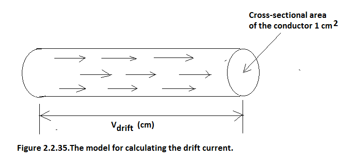
Refer to Figure 2.2.35.
J drift │ e (drift current due to holes) = number of coulombs of electron charge passing through the unit cross-sectional area per unit time
=q×n(electrons/cc)×v drift (cm)×1(cm 2 )
Therefore J drift │ e =qnv drift │ e (2.2.7.5)
J drift │ hole =qnv drift │ hole (2.2.7.6)
Total Drift Current J Drift = qnv drift │ e + qnv drift │ hole (2.2.7.7)
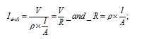
J Drift = qnμ n E+ qnμ p E = (qnμ n + qnμ p )E =σE (2.2.7.7)
Where conductivity of the Si-Rod σ(Siemens/cm) = (qnμ n + qnμ p )(2.2.7.8)
But σ = 1/ρ and E = V/l where V=applied Voltage across the sample and l=length of the sample.
Therefore Eq.(2.2.7.7) is rewritten as:
I drift /A(cross-sectional area of the Si-Rod)=(1/ρ)×(V/l)(2.2.7.9)
Hence Eq.(2.2.7.9) is rearranged as:
Eq.(2.2.7.10) is in fact Ohm’s Law.
2.2.7.3. Scatter Limited Velocity.
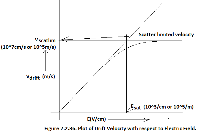
At low fields, after every scattering electron manages to transfer its excess energy to the lattice and electron gets reset. But as drift velocity approaches Thermal Velocity =√(3kT/m e )=10 7 cm/s the quasi equilibrium position becomes unachievable and electron’s drift velocity saturates at scatter-limited velocity which is same as the thermal velocity 10 7 cm/s. This occurs at E = 10 3 /cm.
From this point onward Ohm’s law is untenable.
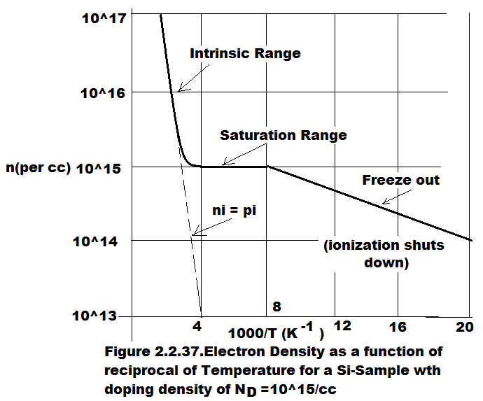
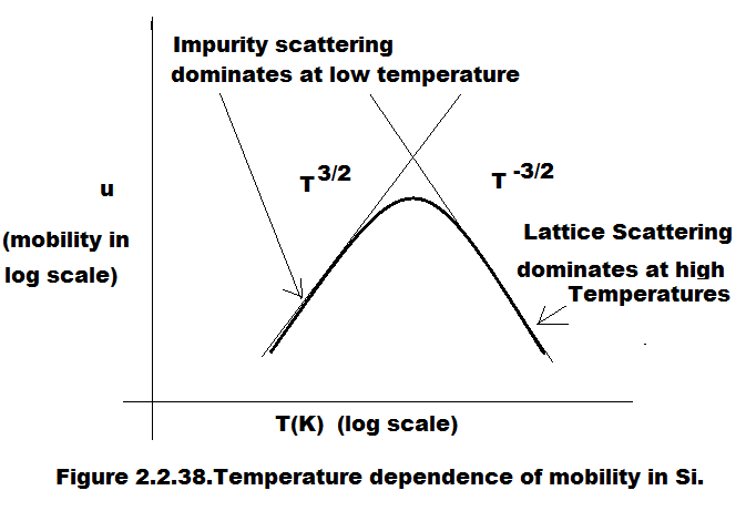
2.2.7.4. Temprature dependence of conductivity of metal and semi-conductor.
Using Eq.(2.2.7.4) the dependence of mobility is as shown in Figure 2.2.38.
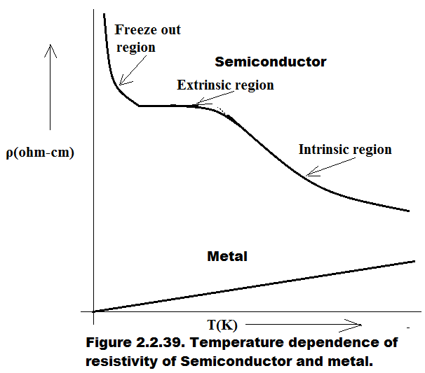
In Figure 2.2.39. the temperature dependence of resistivity of Extrinsic Semiconductor and Metal are shown. By inspection of the Figure we find that Metal has a positive temperature coefficient of resistance whereas Semiconductor has negative temperature coefficient of resistance in intrinsic dominated region. In freeze out region its resistivity approaches that of an insulator.
Notification Switch
Would you like to follow the 'Solid state physics and devices-the harbinger of third wave of civilization' conversation and receive update notifications?

|
|

|
|

|
|

|
|

|
|

|
|

|
|

|
|

|
|

|