

| << Chapter < Page | Chapter >> Page > |
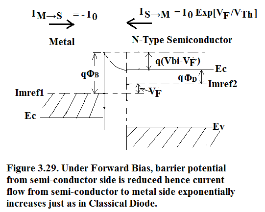
Under no bias, there is equal current flowing across the potential barrier from two sides. Hence there is detailed charge balance is maintained and net current across the Schottky Barrier is zero.
The Barrier Potential seen from the metal side is Φ B and remains unchanged even under bias condition. Hence current from Metal to Semiconductor is kept at -I 0 under forward as well as reverse biased condition..
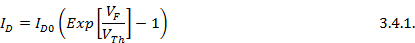
But the Barrier Potential from the semiconductor side is (V bi -V F ) under forward bias condition just as in Classical Diode and as shown in Figure 3.29. Hence carrier diffuses across the forward biased junction with a greater ease and the current from Semiconductor to Metal is I 0 Exp[V F /V Th ]. Therefore net current across the junction under forward bias condition is:
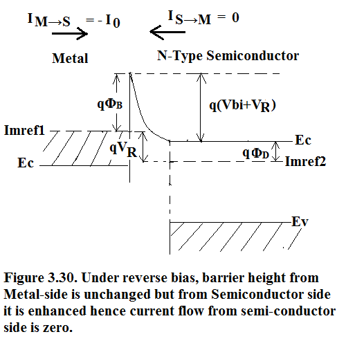
Under reverse bias condition, the barrier potential from Metal-side is unchanged but from the Semiconductor-side it is (V bi +V F ) as shown in Figure 3.30. Hence electron diffusion across the enhanced potential barrier is completely stopped and net current across the junction is:

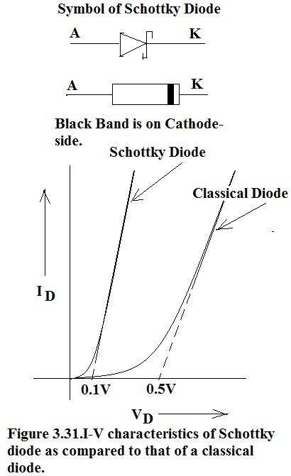
Equation 3.4.1 and Equation 3.4.2 show that Schotky diode behaves exactly like a classical Diode except for a lower knee Voltage at 0.1V because of a reduced barrier potential.
Detailed analysis of Schittky Diode will be done in Supplementary Sheets.
As shown in Section 3.4.1, there is no minority carrier involved in the diode action. It is electron bothways. Hence there is no minority carrier storage and hence as we will see in the switching transients we are never confronted with mionority carrier storage delay in switching transients. Therefore Schottky Diode is known as ‘Hot-Electron Diode’.
It has a lower cut-in voltage of 0.1V because of lower barrier potential. And it has much lower junction plus diffusion capacitance. In Table 3.4.2.1. comparative data sheets of a Schottky Diode 1N5711 and Classical Diode 1N4001 are given.
Low fotward voltage drop and fast switching makes it ideal for protection of MOS devices, steering, biasing and coupling diodes for fast switching and low logic level application. It has higher cut-off frequency, it is reproducible and it has ease of fabrication.
In Figure 3.31, its symbol and I-V characteristics in comparison to I-V characteristics of a classical diode is shown.
Table 3.4.2.1. Comparative Data Sheets of Schottky Diode 1N5711 and Classical Diode 1N4001.
| 1N5711(Schottky Diode) | 1N4001(Classical Diode) | ||||
|---|---|---|---|---|---|
| PIV | 70V | PIV | 50V | ||
| P D | 400mW | P D | 500mW | ||
| I D0 | 200nAAt V R =-50V | I D0 | 5μAAt V R =-50V | ||
| V γ | 0.1V | At 10μA | V γ | 0.5V | At 10μA |
| V F | 0.4V | At 1mA | V F | 0.65V | At 1mA |
| C Tot | 2pF | 20pF | |||
| t rr (ReverseRecovery time) | 1ns | 3μs |
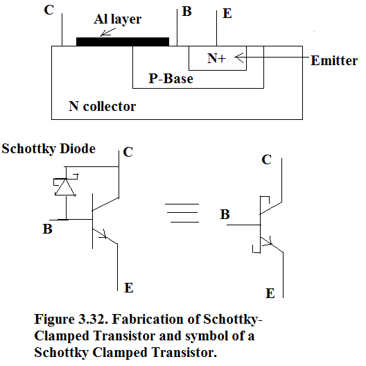
TTL Gate (Transistor-Transistor Logic)74Series is the most commonly used Saturating Logic Family. It suffered from a serious drawback and that was of SPEED. TTL under HIGH conditiont is in cut-off region and in LOW condition it is in deep-saturation. While switching from LOW to HIGH, it suffered from considerable storage delay because of deep-saturation and because of excessive minority carrier storage in the BASE in saturation mode. But if we put a Schottky Diode in parallel to BC Juncttion then even before BC junction is fully forward biased Schottky Diode is turned on.This prevents the BJT from going into deep saturation. A Schottky Clamped Transistor as shown in Fig 3.32. is barely saturated when it goes to LOW condition. Therefore it quickly comes out of Saturation Region and moves to Cut-Off region.This considerably improves the switching speed and toggle rate. The cross-section and the symbol of a Schottky Clamped Transistor used in TTL gate is shown in Figure 3.32. Such a TTL gate is known as Schottky Clamped TTL in 74AS series.
3.5. Ohmic Contact.
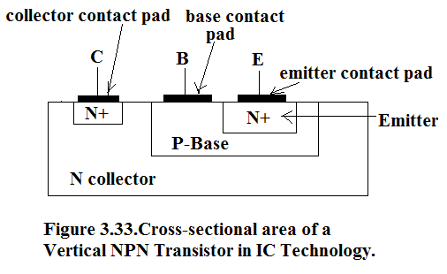
Aluminum contact pad to P-Type semiconductor is an ohmic contact but Aluminum contact pad to N-Type semiconductor is a rectifying contact which we have seen to be Schottky Diode as seen in Figure 3.32. In Si-ICs, ohmic contact to N-Type Collector is never made directly. First a N+ contact region is diffused in N Collector and then Al contact pad is deposited on N+ contact region as shown in Figure 3.33.
In nanotechnology era, greater care is taken in making contact with N-semiconductor as show in Figure 3.34.
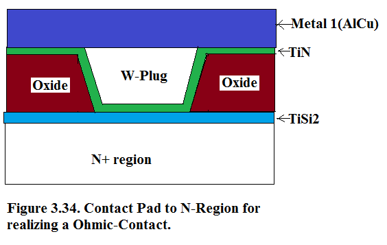
As seen in Figure 3.34. upper layer of heavily doped N+ region is converted into Titanium Silicide. Over this Silicide layer, Oxide layer is deposited. A contact hole is made in Oxide Layer to reach Titanium Silicide. A thin layer of Titamium Nitride is deposited lining the contact hole. This prevents the reaction and inter-diffusion between Silicide and Tungsten Plug.Tungsten Plug is deposited by CVD to fill the contact hole. Over the Tungsten Plug a layer of Metal(Al with some minute quantity of Cu) is deposited to make contact with the underlying N+ region via the tungsten Plug. This gives an ideal ohmic contact.
Notification Switch
Would you like to follow the 'Solid state physics and devices-the harbinger of third wave of civilization' conversation and receive update notifications?

|
|

|
|

|
|

|
|

|
|

|
|

|
|

|
|

|
|
|
|