

| << Chapter < Page | Chapter >> Page > |
In 1874, Braun noted the dependency of total resistance on the polarity of the applied voltage and on the surface conditions. By 1904, point contact diodes started coming into practical use. These were known as ‘Cat Whiskers’ used in crystal diode in demodulating the AM Radio Broadcast Signals. In 1931, Wilson gave the transport theory based on the Band Theory of Solids. In 1938, Schottky suggested that contact potential could develop at metal-semiconductor interface. The model based on this is known as Schottky Model. In 1938, Mott gave the model for swept-out Metal-Semiconductor contact. This is known as Mott barrier. In 1957, Henish in his book ‘Rectifying Semiconductor Contacts’ summarized the basic theory and the historical development of rectifying Metal-Semiconductor Contacts.
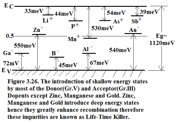
Table.3.4.1.Position of III and V elements energy states within the band-gap of Silicon.
The energy values refer to the energy below conduction bandedge in case of donor and refer to the energy above valence bandedge in case of acceptor .
[Reference: ‘Semiconductor Devices-basic principles’, by Jasprit Singh, Chapter 2,pp 74, 2007 reprint, Wiley –India Publication]
| Semiconductor | Impurity(Donor) | E d (meV) | Impurity(Acceptor) | E a (meV) |
|---|---|---|---|---|
| Si | Li | 33 | B | 45 |
| Sb | 39 | Al | 67 | |
| P | 45 | Ga | 72 | |
| As | 54 | In | 100 | |
| Mn(deep EnergyStates) | 530 | Au(deep EnergyStates) | 540 | |
| Zn(deep EnergyStates) | 550 |
Deep energy states in the band-gap act as the effective stepping stone for recombination hence they act as the Life-Time killer. Their introduction will lead to reduction in minority carriers storage under forward bias condition.Hence in 70s to reduce the storage delay time, Gold was introduced as the life-time killer. But subsequently this was discarded and Schottky Clamped transistors were used to reduce the minority carrier storage delay. Nowadays Schottky-clamped TTL gates have become the norm of the day. These are available as 74AS series.
Aluminum layer on N-Type Semiconductor forms a rectifying junction with a built-in barrier potential as shown in Figure 3.27. and Figure 3.28.
In Figure 3.27. Case (a):
Work-function of Metal=qΦ m (eV).
Work-function of Siliconl=qΦ Si (eV).
Electron affinity in Silicon=χ Si (eV).
Barrier Potential Energy seen from metal side = qΦ B =q(Φ m -χ Si ).
Barrier Potential seen from semi-conductor side =V bi = (Φ m -Φ Si ).
Built-in Barrier Potential on the semi-conductor side can be expressed as= V bi = (Φ B -Φ D ).
These are in ideal condition. In real – life, there are surface states at the interface which complicate the situation and measured values of Φ B are much greater than the theoretical values. Table 3.4.1. gives the measured Schottky Barrier heights for electrons on N-type Silicon Φ B │ N and the measured Schottky Barrier heights for holes on P-type Silicon Φ B │ P
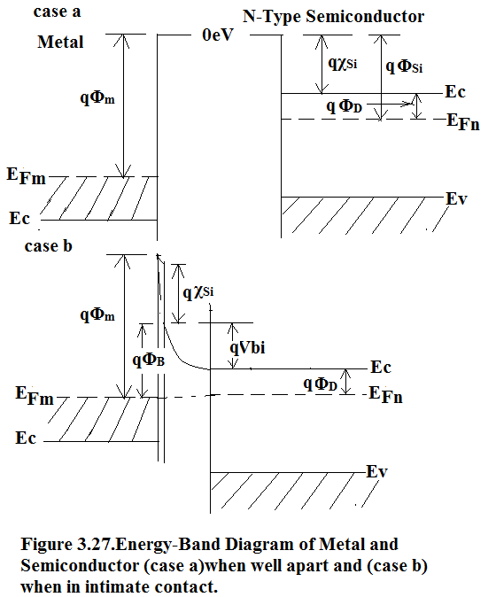
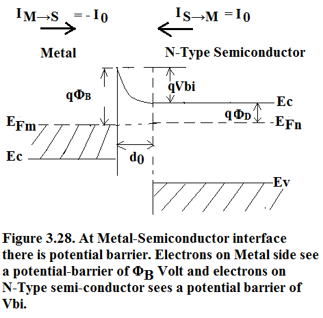
Table 3.4.1. Measured Schottky Barrier heights for electrons on N-type Silicon Φ B │ N and the measured Schottky Barrier heights for holes on P-type Silicon Φ B │ P .
| Metal | Mg | Ti | Cr | W | Mo | Pd | Au | Pt |
|---|---|---|---|---|---|---|---|---|
| Φ M (eV) | 3.7 | 4.3 | 4.5 | 4.6 | 4.6 | 5.1 | 5.1 | 5.7 |
| Φ B │ N (eV) | 0.4 | 0.5 | 0.61 | 0.67 | 0.68 | 0.77 | 0.8 | 0.9 |
| Φ B │ N (eV) | - | 0.61 | 0.50 | - | 0.42 | - | 0.3 | - |
Notification Switch
Would you like to follow the 'Solid state physics and devices-the harbinger of third wave of civilization' conversation and receive update notifications?

|
|

|
|

|
|

|
|

|
|

|
|

|
|

|
|

|
|

|