

| << Chapter < Page | Chapter >> Page > |
The PCB pads are thin and most often do not provide enough solder for connecting the SMD component. Before placing the SMD component on the board, one should flux and lightly tint each tab. To do this, take a toothpick or similar object and deposit and ever so slight amount of flux on each pad. Next, place the tip of the soldering iron in the tinning paste, remove and clean on the sponge. Now touch the tip to a strand of solder and tin-up the tip of the iron. Focus in on the tabs and bring the tip of the iron over one of the tabs. Touch the tip of the iron to the tab and slight rub the tip over the tab to deposit a thin layer of solder that should bond with the board tab. Do this to each tab. Now take a pair of tweezers and hold the SM component in place. Bring the tip of the iron to one edge of the tab and melt the solder. Figure 3 illustrates the tab for each pin of the MSP430F449 soldered onto the board.

Do not touch the tip to the SMD component. As the solder on the tab melts, the solder on the tip of the SMD component will also melt. In order to observe all this, a microscope will be needed. Remove the tip of the iron but hold the component in place, momentarily, for the solder to cool and set. Remove the tweezers and repeat the process at the other end of the component. Most often there is a good bond and no further soldering is required. Furthermore, there is a slight change in the procedure for mounting polarized capacitors. This slight change is illustrated in Figure 4.

Also, on many polarized capacitors the two small solder tabs have the same size. In this case the backside of the capacitor will have a small stripe to indicate the + (positive) terminal of the capacitor. One should always check the source catalog for this information if it is not clear which side is positive.
The MSP 430F449 is a very fine-pitch chip. That is, the connect point to the chip are numerous and very close together. There are 25 connect points on each side of the chip. The chip is roughly 1/2 inch on each side. That is, one is looking at roughly 25 connect points spread over 1/2 of an inch. To mount the MSP 430 to the PCB requires some tedious soldering work.
Start by placing the board on the microscope with the base light and top light of the microscope turned on. This provides heat to the board that will be helpful in the fluxing process. Consider the diagram of Figure 3 that represents the portion of the PCB where the MSP 430 will be mounted.
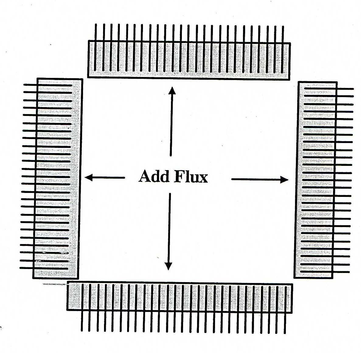
The student should take an appropriate object such as a toothpick with flux on the tip and place the flux in the shaded areas shown on the circuit traces of Figure 5. Next, place the MSP 430 on the trace pattern above with the MSP 430 centered all-around. This takes a little time. Be careful to align the connect points to the PCB completely around the MSP 430. The notch on the bottom left corner of the MSP 430F indicates the placement of the first pin.

Notification Switch
Would you like to follow the 'Eel3111 force sensor group july 2010' conversation and receive update notifications?

|
|

|
|

|
|

|
|

|
|

|
|

|
|

|
|

|
|
|
|