<< Chapter < Page Chapter >> Page >
SSPD_Chapter 7_Part 6_Basic Circuit Concepts_continued 3 calculates the rise time and the fall timne and proves that for symmetric switching PMOS width must be 2.5 times wider than NMOS width.

SSPD_Chapter 7_Part 6_Basic Circuit Concepts_continued 3

7.6.4. Formal Estimation of CMOS Inverter delay.

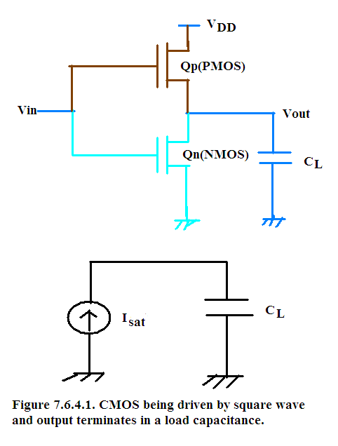
In Figure 7.6.4.1 we show a CMOS Inverter being driven by square wave and loaded with input capacitance of the subsequent stage. We model the CMOS Inverter during switching transients by constant current source driving the load capacitance.

The switching transient is shown in Figure 7.6.4.2.

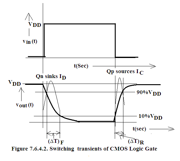
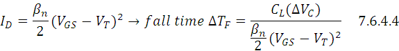
As can be seen in Figure 7.6.4.2, during HIGH to LOW switching NMOS (Q n ) provides the low impedance path to ground and hence sinks the discharge current. Hence saturation current of NMOS provides the I D .

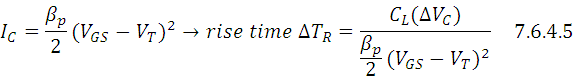
Similarly during LOW to HIGH switching PMOS (Q p ) provides the low impedance path from V DD bus to the load capacitance and hence sources the charging current. Hence saturation current of PMOS provides the I C .

Referring to the circuit model in Figure 7.6.4.1 we see that:

Rate of change of capacitance voltage = Constant Current/C

Therefore:

Therefore:

Therefore:

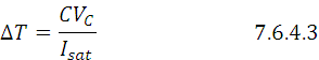
During output HIGH to LOW transient: NMOS (Q n ) is sinking the current from the load capacitance hence constant current source is a discharge current I D coming as the saturation current of NMOS where

During output LOW to HIGH transient:PMOS(Q p ) is sourcing the current to the load capacitance hence constant current source is a charging current I C coming as the saturation current of PMOS where

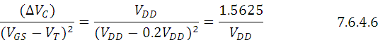
But ∆V C = V DD , V GS = V DD and V T = 0.2 V DD therefore

Substituting Eq.7.6.4.6 in Eq 7.6.4.4 and Eq.7.6.4.5 we get:

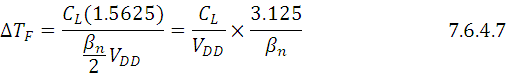
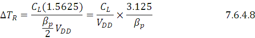
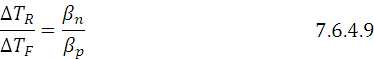
Dividing Eq 7.6.4.8 by Eq.7.6.4.7 we get:

From Basic Electrical Properties we know that

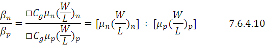
From Device Physics we know that

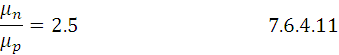
We also know from section 7.3.12 titled ‘optimization of geometric parameters to achieve the beswt CMOS performance’ that :

Substituting the two conditions stated by Eq.7.6.4.8 and Eq.7.6.4.9 in Eq 7.6.4.7 we get

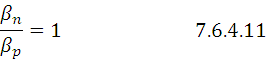
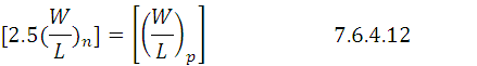
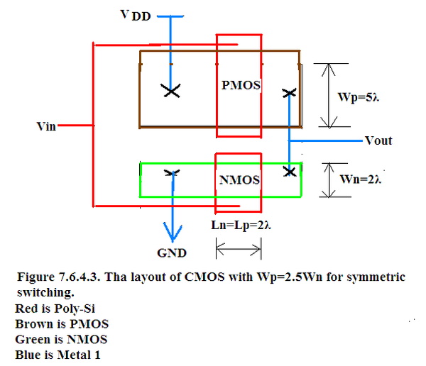
Eq 7.6.4.10 implies that we will get symmetric switching transients as well as maximum Noise Margin if satisfy the condition stated in Eq 7.6.4.11 namely

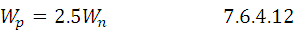
Hence CMOS layout will be as shown in Figure 7.6.4.3 for optimum performance in all sense of the word i.e in the sense of switching transient and in the sense of noise margin.

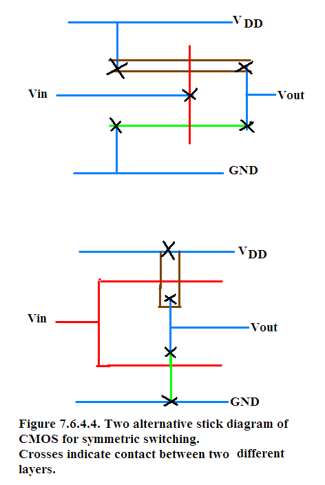
Two alternative layouts are shown in Figure 7.6.4.4.

In all the three figures, where metal has to connect to Poly-Si or to n-channel or to p-channel there a contact has to be made symbolized by black cross.

Questions & Answers

what does preconceived mean
sammie Reply
physiological Psychology
Nwosu Reply
How can I develope my cognitive domain
Amanyire Reply
why is communication effective
Dakolo Reply
Communication is effective because it allows individuals to share ideas, thoughts, and information with others.
effective communication can lead to improved outcomes in various settings, including personal relationships, business environments, and educational settings. By communicating effectively, individuals can negotiate effectively, solve problems collaboratively, and work towards common goals.
it starts up serve and return practice/assessments.it helps find voice talking therapy also assessments through relaxed conversation.
miss
Every time someone flushes a toilet in the apartment building, the person begins to jumb back automatically after hearing the flush, before the water temperature changes. Identify the types of learning, if it is classical conditioning identify the NS, UCS, CS and CR. If it is operant conditioning, identify the type of consequence positive reinforcement, negative reinforcement or punishment
Wekolamo Reply
please i need answer
Wekolamo
because it helps many people around the world to understand how to interact with other people and understand them well, for example at work (job).
Manix Reply
Agreed 👍 There are many parts of our brains and behaviors, we really need to get to know. Blessings for everyone and happy Sunday!
ARC
A child is a member of community not society elucidate ?
JESSY Reply
Isn't practices worldwide, be it psychology, be it science. isn't much just a false belief of control over something the mind cannot truly comprehend?
Simon Reply
compare and contrast skinner's perspective on personality development on freud
namakula Reply
Skinner skipped the whole unconscious phenomenon and rather emphasized on classical conditioning
war
explain how nature and nurture affect the development and later the productivity of an individual.
Amesalu Reply
nature is an hereditary factor while nurture is an environmental factor which constitute an individual personality. so if an individual's parent has a deviant behavior and was also brought up in an deviant environment, observation of the behavior and the inborn trait we make the individual deviant.
Samuel
I am taking this course because I am hoping that I could somehow learn more about my chosen field of interest and due to the fact that being a PsyD really ignites my passion as an individual the more I hope to learn about developing and literally explore the complexity of my critical thinking skills
Zyryn Reply
good👍
Jonathan
and having a good philosophy of the world is like a sandwich and a peanut butter 👍
Jonathan
generally amnesi how long yrs memory loss
Kelu Reply
interpersonal relationships
Abdulfatai Reply
What would be the best educational aid(s) for gifted kids/savants?
Heidi Reply
treat them normal, if they want help then give them. that will make everyone happy
Saurabh
What are the treatment for autism?
Magret Reply
hello. autism is a umbrella term. autistic kids have different disorder overlapping. for example. a kid may show symptoms of ADHD and also learning disabilities. before treatment please make sure the kid doesn't have physical disabilities like hearing..vision..speech problem. sometimes these
Jharna
continue.. sometimes due to these physical problems..the diagnosis may be misdiagnosed. treatment for autism. well it depends on the severity. since autistic kids have problems in communicating and adopting to the environment.. it's best to expose the child in situations where the child
Jharna
child interact with other kids under doc supervision. play therapy. speech therapy. Engaging in different activities that activate most parts of the brain.. like drawing..painting. matching color board game. string and beads game. the more you interact with the child the more effective
Jharna
results you'll get.. please consult a therapist to know what suits best on your child. and last as a parent. I know sometimes it's overwhelming to guide a special kid. but trust the process and be strong and patient as a parent.
Jharna
Got questions? Join the online conversation and get instant answers!
Jobilize.com Reply

Get Jobilize Job Search Mobile App in your pocket Now!

Get it on Google Play Download on the App Store Now


Source:  OpenStax, Solid state physics and devices-the harbinger of third wave of civilization. OpenStax CNX. Sep 15, 2014 Download for free at http://legacy.cnx.org/content/col11170/1.89
Google Play and the Google Play logo are trademarks of Google Inc.

Notification Switch

Would you like to follow the 'Solid state physics and devices-the harbinger of third wave of civilization' conversation and receive update notifications?

Ask