

| << Chapter < Page | Chapter >> Page > |
SSPD_Chapter 7_Part 6_Basic Circuit Concepts.
7.6.1. Sheet Resistance.
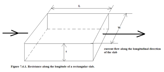
Referring to Figure 7.6.1 we see that:
Resistance of the slab along the longitudinal axis:

Therefore

Table 7.6.1 gives the typical values of the sheet resistance of the different layers of CMOS IC circuit.
Table 7.6.1.Typical values of the sheet resistance R S of MOS layers for technology generation 5μm, 2μm and 1.2μm. (Here 5μm, 2μm and 1.2μm imply the minimum feature size = channel length for the given technology . Consequently λ is 2.5μm, 1μm and 0.6μm for these three generations respectively).
| Layer | R S (Ω/square) | ||
| 5μm | 2μm | 1.2μm | |
| Metal | 0.03 | 0.04 | 0.04 |
| Diffusion | 10→50 | 20→45 | 20→45 |
| Silicide | 2→4 | ||
| Poly_Si | 15→100 | 15→30 | 15→30 |
| N channel | 10 4 | 2×10 4 | 2×10 4 |
| P channel | 2.5×10 4 | 4.5×10 4 | 4.5×10 4 |
7.6.1.1. Resistance calculation of N-Channel in 5μm Generation of Technology.
If L:W = 2λ:2λ then R channel = R sheet ×(L/W) = 1×10 4 Ω..
If L:W = 8λ:2λ then R channel = R sheet ×(L/W) = 1×10 4 Ω.×4 =4×10 4 Ω..
With scaling, feature size has decreased and the pitch of metal interconnect has decreased. This has led to excessive RC time delay. To control this, metal interconnects are being replaced by Metal Silicides. The metal silicides or the refractory silicides are formed by depositing metal on poly-silicon and then sintering it. Though these have proved to be successful substitutes of metal interconnects the extra processing steps make it uneconomical.
With scaling the cross-sectional area of the metal interconnect decreases and current density increases. As this exceeds the limit of 1.5mA/mm, metal grains are pushed around and wire interconnects break. This is called migration. Silicides prevent electron migration.
With the latest generation of technology, silicides are being further replaced by copper interconnects.
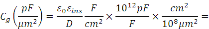
7.6.2. Area Capacitance of Layers.
Parallel plate capacitance is given by the formula:
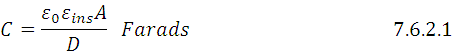
Where D=thickness of the dielectric between the plates;
A = cross-sectional area of the plate;
Absolute permittivity (permittivity) = ε 0 = 8.85×10 -14 F/cm;
Relative permittivity of the dielectric in this case SiO 2 = 3.9;
In VLSI design we express Capacitance per unit area = (pF/μm 2 ). To obtain it in this form we have to the scaling factor as follows:
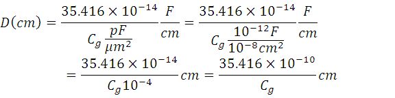
But Gate-to-Channel capacitance, C g (pF/μm 2 ) = 4×10 -4 , 8×10 -4 , 16×10 -4 ;
Therefore D = 88.5nm, 44.27nm, 22.1nm
Typical values are given in Table 7.6.2.
Table 7.6.2. Typical area capacitance values for MOS cuircuits.
| Capacitance | Value in pF×(10 -4 /μm 2 ) (relative value in brackets) | ||
| 5μm | 2μm | 1.2μm | |
| Gate Oxide Thickness | 88.5nm | 44.27nm | 22.1nm |
| Gate to Channel | 4 (1.0) | 8 (1.0) | 16 (1.0) |
| Difusion(active) | 1 (0.25) | 1.75 (0.22) | 3.75 (0.23) |
| Poly-Si to substrate | 0.4 (0.1) | 0.6 (0.075) | 0.6 (0.038) |
| Metal 1 to substrate | .3 (0.075) | 0. 33 (0.04) | 0.33 (0.02) |
| Metal 2 to substrate | 0.2 (0.05) | 0.17 (0.02) | 0.17 (0.01) |
| Metal 2 to metal 1 | 0.4 (0.1) | 0.5 (0.06) | 0.5 (0.03) |
| Metal 2 to poly-Si | .3 (0.075) | 0. 3 (0.038) | 0.3 (0.018) |
Notification Switch
Would you like to follow the 'Solid state physics and devices-the harbinger of third wave of civilization' conversation and receive update notifications?

|
|

|
|

|
|

|
|

|
|

|
|

|
|

|
|

|
|

|