

| << Chapter < Page | Chapter >> Page > |
These masks have been described in the sequence in which they will be used during actual fabrication. These masks are used to impart selectivity to different processes of fabrication by photo-resist process or photolithography.
The photoresist process consists of the following basic operation:
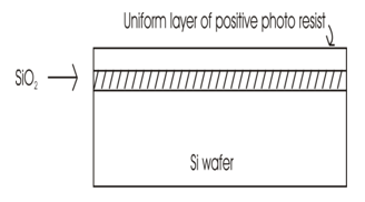
(1) A uniform layer of light sensitive photo resistive emulsion is coated over the wafer by a spinner machine.
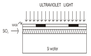
(2) In a mask alignment and ultraviolet exposure machine, the photo-mask used, corresponding to the fabrication step in question, is correctly aligned with respect to the previous pattern on wafer. Next photo-mask is brought in intimate contact with photo resist layer and the photo resist layer is exposed to intense ultraviolet light for a given stipulated time through the photo-mask. The KPR layer is baked in an oven at 100°C to dry it. As the lateral feature size has decreased from generation to generation, so has the exposure method changed and the wavelength of the exposing light has been progressively decreased so as to satisfy the Rayleigh Equation. In 1997, 0.35µm Technology used 248 nm Deep Ultra Violet light. As we moved to 0.15µm Technology we used 193µm DUV light. Today as we adopt 0.045µm Technology we are using DUV 193 µm immersion Technique. The Contact Printing gave way to Proximity Printing and Proximity Printing gave way to Projection Printing. Today we are using Deep UltraViolet (193nm) Immersion Technique.[For detailed discussion see “Journey of IC Technolgy from micro to nano Era- Part 3”.]
(3) By photo resist developer, the image of the mask is developed in the photo resist layer . In positive photo resist the exposed layer gets removed leaving the wafer surface bare in those areas. In negative photo resist the unexposed layer remains soft and is dissolved away by the developer.
(4) By baking the wafers in baking oven at a given temperature for a given time, the remaining photo resist pattern on the wafer is fixed and becomes resistant to corrosive etches.
(5) Depending on the fabrication step, either SiO 2 or Aluminum layer on the substrate (or wafer) is etched through the photo resist pattern carving out an identical pattern on the surface of the substrate. Hydrogen Flouride (HF) is used for etching SiO 2 and Sodium Hydroxide (NaOH) is used for etching Aluminum layer. Hydrogen Fluoride is highly corrosive and is stored in Teflon beaker. Teflon tweezers are used to handle the wafers and Teflon gloves have to be used by the worker to protect himself from Hydrogen Flouride.
(6) Next by stripper ,the hardened photo resist pattern is stripped and the wafer are cleaned for the next fabrication step.
Photolithographic processes are illustrated in Fig (6.3)
Notification Switch
Would you like to follow the 'Solid state physics and devices-the harbinger of third wave of civilization' conversation and receive update notifications?

|
|

|
|

|
|

|
|

|
|

|
|
|
|
|
|
|
|

|
|

|