<< Chapter < Page Chapter >> Page >
This Appendix is based on the patent filed in US for a simplified method of fabricating poly-silicon emitter BJT.

Appendix V

Analysis of Polysilicon emitter BJT .

In Polysilicon emitter BJT (PET), a polycrystalline Si Film lies between Metallic Emitter Contact and Silicon Proper. By ion-implantation, the Polycrystalline Silicon Film is doped with Donor Arsenic Ions. By subsequent annealing, shallow diffusion of Donor Arsenic atoms from N + Poly-Silicon Source takes place leading to a shallow layer of N + in Si proper contacted by a similarly doped N + Poly-Silicon thin film. This structure is known as Polysilicon emitter BJT.

This is suitable for shallow EB Junction;

Compatible with self-aligned processing. This minimizes parasitic Resistance and Capacitances leading to faster response time.

Short Circuit Current Gain (β F ) in PET is considerably improved as compared to that of shallow all crystalline emitter of equivalent thickness.

The physics of improvement of Short Circuit Current Gain (β F ) in PET.

Figure V.1. Minority Carrier Concentration in a shallow EB Junction case 1. All pure single crystal structure and case 2 in Poly Si Emitter BJT.

Since W E <<L pE , therefore there is negligible recombination through out the Emitter. At the interface of Poly Si(region 1) and Pure Si(Region 2), continuity of carrier concentration and continuity of diffusion current requires that:

=

Therefore carrier concentration gradient in poly Si region is several times the carrier concentration gradient in Pure Silicon Emitter because mobility of hole in Pure Single Crystal Silicon region is several times greater than that in Poly Si on account of domain scattering in Poly region. Hence hole current crossing EB junction into Emitter is considerably reduced leading to a near unity Injection Efficiency. This leads to a much better α and hence a much better β . Now doping of base can be increased leading to a reduced base spreading resistance and hence better Figure of Merit and better Frequency Response without losing on current gain.

Process Steps of Poly Si Emitter BJT US Patent5736447. (P + NP)

www.patentsform.us/patents/5736447/fulltext.html

Step 1. Ion-Implantation of N type Base in P type substrate. Base Region is in space-apart relationship to the collector region.

Step 2. Stripping of exposed KPR layer(104) and deposition of FIRST Insulation Layer.

Step 3. Etching out of Emitter Contact Hole. The oxide film (108) is first isotropically etched and then anisotropically etched or we could do anisotropic etching directly

Step 4.Deposition of first conducting layer of thickness 500 to 2000 Angstrom. The first conducting layer is Poly-Silicon layer or in-situ polySi. P-type impurities namely Boron Ions are Ion-Implanted into the first conducting layer. Ion-Implantation energy is 50 to 100keV and the dose is 2×10 15 - 6×10 17 ions/cm 2 . Ion-implanted poly-Si layer acts as the source for shallow diffusion of P-type impurities in N-type Base to form a shallow self aligned Emitter in Pure Single Crystal Silicon Substrate. This shallow diffusion is achieved by rapid thermal annealing(RTA) at a temperature above 600ºC in a nitrogen atmosphere at a temperature of 800ºC - 950ºC.

Step 5. Base and Collector contact holes etched out in first conducting layer(110) and in first insulating layer(108) to Base(106) and to Collector(102). This is achieved by isotropic and then anisotropic etching or only by anisotropic etching.

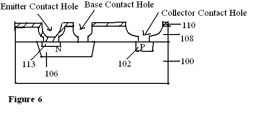
Step 6. Second Conducting Layer is deposited over 110 and to fill the contact holes at Emitter, Base and Collector. It may be Poly-Si or poly-Si in-situ or Metal Silicide. Second Conducting layer plus underlying conducting layer are patterned into Emitter Contact Pad, Base Contact Pad and Collector Contact Pad.

Directly quoted from the Patent:

“The above-described method of the present invention results in a BJT having a thin or shallow emitter region 113 which effectively minimizes the base-emitter junction capacitance, without the need for additional photolithographic steps required by the presently available technology. In this regard, the polysilicon emitter 112 is formed simultaneously with the patterning of the first and second conductive layers and is self –aligned with the resultant emitter contact. Moreover the necessity of the oxide layer 38 of the conventional method for manufacturing a BJT is eliminated. Hence this method is less complex and less costly than the conventional method”.

Questions & Answers

what does preconceived mean
sammie Reply
physiological Psychology
Nwosu Reply
How can I develope my cognitive domain
Amanyire Reply
why is communication effective
Dakolo Reply
Communication is effective because it allows individuals to share ideas, thoughts, and information with others.
effective communication can lead to improved outcomes in various settings, including personal relationships, business environments, and educational settings. By communicating effectively, individuals can negotiate effectively, solve problems collaboratively, and work towards common goals.
it starts up serve and return practice/assessments.it helps find voice talking therapy also assessments through relaxed conversation.
miss
Every time someone flushes a toilet in the apartment building, the person begins to jumb back automatically after hearing the flush, before the water temperature changes. Identify the types of learning, if it is classical conditioning identify the NS, UCS, CS and CR. If it is operant conditioning, identify the type of consequence positive reinforcement, negative reinforcement or punishment
Wekolamo Reply
please i need answer
Wekolamo
because it helps many people around the world to understand how to interact with other people and understand them well, for example at work (job).
Manix Reply
Agreed 👍 There are many parts of our brains and behaviors, we really need to get to know. Blessings for everyone and happy Sunday!
ARC
A child is a member of community not society elucidate ?
JESSY Reply
Isn't practices worldwide, be it psychology, be it science. isn't much just a false belief of control over something the mind cannot truly comprehend?
Simon Reply
compare and contrast skinner's perspective on personality development on freud
namakula Reply
Skinner skipped the whole unconscious phenomenon and rather emphasized on classical conditioning
war
explain how nature and nurture affect the development and later the productivity of an individual.
Amesalu Reply
nature is an hereditary factor while nurture is an environmental factor which constitute an individual personality. so if an individual's parent has a deviant behavior and was also brought up in an deviant environment, observation of the behavior and the inborn trait we make the individual deviant.
Samuel
I am taking this course because I am hoping that I could somehow learn more about my chosen field of interest and due to the fact that being a PsyD really ignites my passion as an individual the more I hope to learn about developing and literally explore the complexity of my critical thinking skills
Zyryn Reply
good👍
Jonathan
and having a good philosophy of the world is like a sandwich and a peanut butter 👍
Jonathan
generally amnesi how long yrs memory loss
Kelu Reply
interpersonal relationships
Abdulfatai Reply
What would be the best educational aid(s) for gifted kids/savants?
Heidi Reply
treat them normal, if they want help then give them. that will make everyone happy
Saurabh
What are the treatment for autism?
Magret Reply
hello. autism is a umbrella term. autistic kids have different disorder overlapping. for example. a kid may show symptoms of ADHD and also learning disabilities. before treatment please make sure the kid doesn't have physical disabilities like hearing..vision..speech problem. sometimes these
Jharna
continue.. sometimes due to these physical problems..the diagnosis may be misdiagnosed. treatment for autism. well it depends on the severity. since autistic kids have problems in communicating and adopting to the environment.. it's best to expose the child in situations where the child
Jharna
child interact with other kids under doc supervision. play therapy. speech therapy. Engaging in different activities that activate most parts of the brain.. like drawing..painting. matching color board game. string and beads game. the more you interact with the child the more effective
Jharna
results you'll get.. please consult a therapist to know what suits best on your child. and last as a parent. I know sometimes it's overwhelming to guide a special kid. but trust the process and be strong and patient as a parent.
Jharna
Got questions? Join the online conversation and get instant answers!
Jobilize.com Reply

Get Jobilize Job Search Mobile App in your pocket Now!

Get it on Google Play Download on the App Store Now


Source:  OpenStax, Solid state physics and devices-the harbinger of third wave of civilization. OpenStax CNX. Sep 15, 2014 Download for free at http://legacy.cnx.org/content/col11170/1.89
Google Play and the Google Play logo are trademarks of Google Inc.

Notification Switch

Would you like to follow the 'Solid state physics and devices-the harbinger of third wave of civilization' conversation and receive update notifications?

Ask