<< Chapter < Page Chapter >> Page >
Diagram of probe and surface interaction in noncontact mode.

Experimental limitations

A common problem seen in AFM images is the presence of artifacts which are distortions of the actual topography, usually either due to issues with the probe, scanner, or image processing. The AFM scans slowly which makes it more susceptible to external temperature fluctuations leading to thermal drift. This leads to artifacts and inaccurate distances between topographical features.

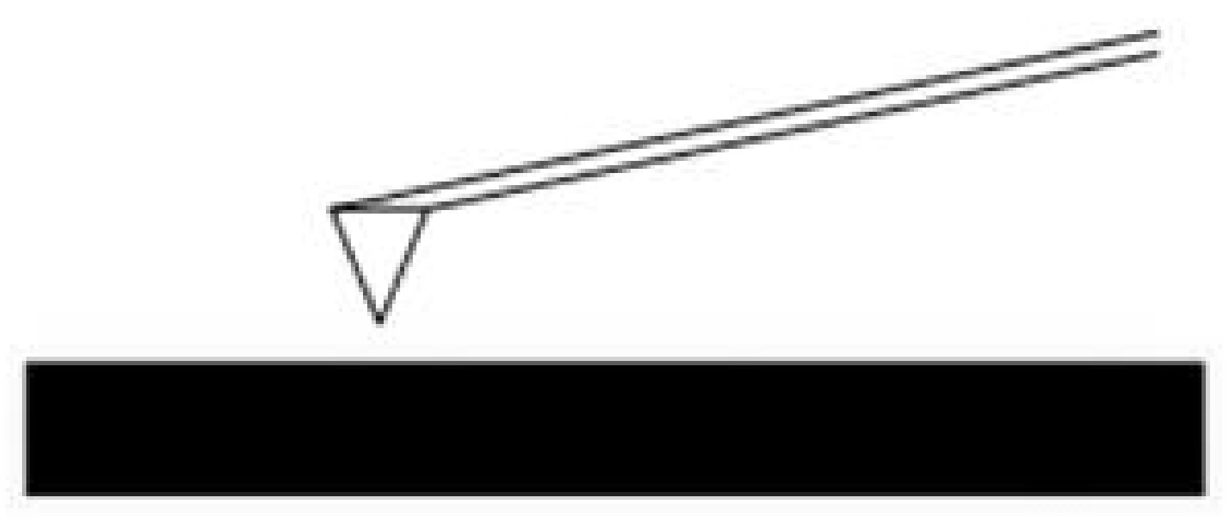
It is also important to consider that the tip is not perfectly sharp and therefore may not provide the best aspect ratio, which leads to a convolution of the true topography. This leads to features appearing too large or too small since the width of the probe cannot precisely move around the particles and holes on the surface. It is for this reason that tips with smaller radii of curvature provide better resolution in imaging. The tip can also produce false images and poorly contrasted images if it is blunt or broken.

The movement of particles on the surface due to the movement of the cantilever can cause noise, which forms streaks or bands in the image. Artifacts can also be made by the tip being of inadequate proportions compared to the surface being scanned. It is for this reason that it is important to use the ideal probe for the particular application.

Sample size and preparation

The sample size varies with the instrument but a typical size is 8 mm by 8 mm with a typical height of 1 mm. Solid samples present a problem for AFM since the tip can shift the material as it scans the surface. Solutions or dispersions are best for applying as uniform of a layer of material as possible in order to get the most accurate value of particles’ heights. This is usually done by spin-coating the solution onto freshly cleaved mica which allows the particles to stick to the surface once it has dried.

Applications of afm

AFM is particularly versatile in its applications since it can be used in ambient temperatures and many different environments. It can be used in many different areas to analyze different kinds of samples such as semiconductors, polymers, nanoparticles, biotechnology, and cells amongst others. The most common application of AFM is for morphological studies in order to attain an understanding of the topography of the sample. Since it is common for the material to be in solution, AFM can also give the user an idea of the ability of the material to be dispersed as well as the homogeneity of the particles within that dispersion. It also can provide a lot of information about the particles being studied such as particle size, surface area, electrical properties, and chemical composition. Certain tips are capable of determining the principal mechanical, magnetic, and electrical properties of the material. For example, in magnetic force microscopy (MFM) the probe has a magnetic coating that senses magnetic, electrostatic, and atomic interactions with the surface. This type of scanning can be performed in static or dynamic mode and depicts the magnetic structure of the surface.

Afm of carbon nanotubes

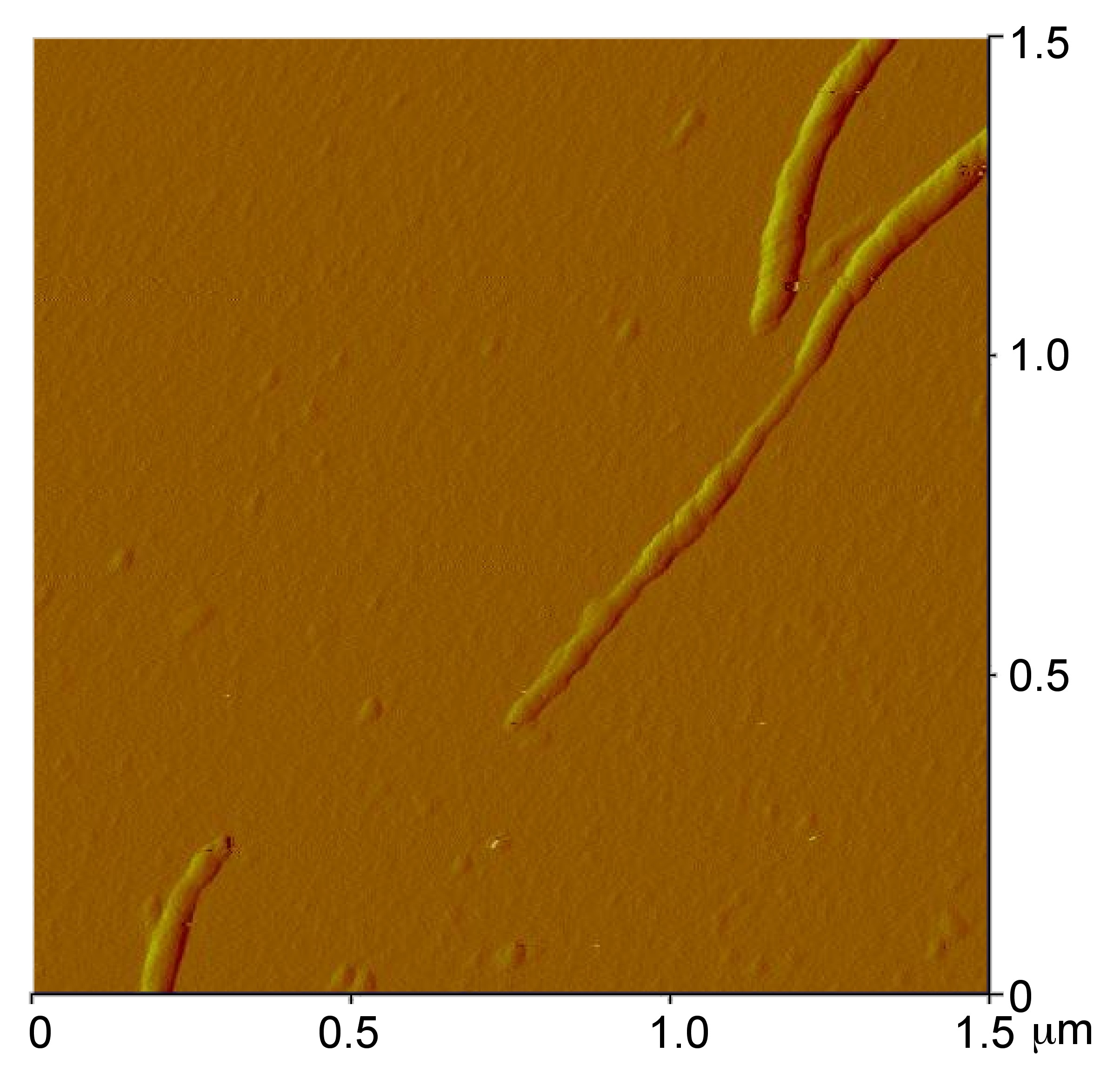
Atomic force microscopy is usually used to study the topographical morphology of these materials. By measuring the thickness of the material it is possible to determine if bundling occurred and to what degree. Other dimensions of the sample can also be measured such as the length and width of the tubes or bundles. It is also possible to detect impurities, functional groups ( [link] ), or remaining catalyst by studying the images. Various methods of producing nanotubes have been found and each demonstrates a slightly different profile of homogeneity and purity. These impurities can be carbon coated metal, amorphous carbon, or other allotropes of carbon such as fullerenes and graphite. These facts can be utilized to compare the purity and homogeneity of the samples made from different processes, as well as monitor these characteristics as different steps or reactions are performed on the material. The distance between the tip and the surface has proven itself to be an important parameter in noncontact mode AFM and has shown that if the tip is moved past the threshold distance, approximately 30 μm, it can move or damage the nanotubes. If this occurs, a useful characterization cannot be performed due to these distortions of the image.

AFM image of a polyethyleneimine-functionalized single walled carbon nanotube (PEI-SWNT) showing the presence of PEI “globules” on the SWNT. Adapted from E. P. Dillon, C. A. Crouse, and A. R. Barron, ACS Nano , 2008, 2 , 156.

Afm of fullerenes

Atomic force microscopy is best applied to aggregates of fullerenes rather than individual ones. While the AFM can accurately perform height analysis of individual fullerene molecules, it has poor lateral resolution and it is difficult to accurately depict the width of an individual molecule. Another common issue that arises with contact AFM and fullerene deposited films is that the tip shifts clusters of fullerenes which can lead to discontinuities in sample images.

Bibliography

  • R. Anderson and A. R. Barron, J. Am. Chem. Soc. , 2005, 127 , 10458.
  • M. Bellucci, G. Gaggiotti, M. Marchetti, F. Micciulla, R. Mucciato, and M. Regi, J. Physics: Conference Series , 2007, 61 , 99.
  • I. I. Bobrinetskii, V. N. Kukin, V. K. Nevolin, and M. M. Simunin. Semiconductor , 2008, 42 , 1496.
  • S. H. Cohen and M. L. Lightbody. Atomic Force Microscopy/Scanning Tunneling Microscopy 2 . Plenum, New York (1997).
  • E. P. Dillon, C. A. Crouse, and A. R. Barron, ACS Nano , 2008, 2 , 156.
  • C. Gu, C. Ray, S. Guo, and B. B. Akhremitchev, J. Phys. Chem. , 2007, 111 , 12898.
  • G. Kaupp, Atomic Force Microscopy, Scanning Nearfield Optical Microscopy and Nanoscratching: Application to Rough and Natural Surfaces . Springer-Verlag, Berlin (2006).
  • S. Morita, R. Wiesendanger, E. Meyer, and F. J. Giessibl. Noncontact Atomic Force Microscopy . Springer, Berlin (2002).

Questions & Answers

what does preconceived mean
sammie Reply
physiological Psychology
Nwosu Reply
How can I develope my cognitive domain
Amanyire Reply
why is communication effective
Dakolo Reply
Communication is effective because it allows individuals to share ideas, thoughts, and information with others.
effective communication can lead to improved outcomes in various settings, including personal relationships, business environments, and educational settings. By communicating effectively, individuals can negotiate effectively, solve problems collaboratively, and work towards common goals.
it starts up serve and return practice/assessments.it helps find voice talking therapy also assessments through relaxed conversation.
miss
Every time someone flushes a toilet in the apartment building, the person begins to jumb back automatically after hearing the flush, before the water temperature changes. Identify the types of learning, if it is classical conditioning identify the NS, UCS, CS and CR. If it is operant conditioning, identify the type of consequence positive reinforcement, negative reinforcement or punishment
Wekolamo Reply
please i need answer
Wekolamo
because it helps many people around the world to understand how to interact with other people and understand them well, for example at work (job).
Manix Reply
Agreed 👍 There are many parts of our brains and behaviors, we really need to get to know. Blessings for everyone and happy Sunday!
ARC
A child is a member of community not society elucidate ?
JESSY Reply
Isn't practices worldwide, be it psychology, be it science. isn't much just a false belief of control over something the mind cannot truly comprehend?
Simon Reply
compare and contrast skinner's perspective on personality development on freud
namakula Reply
Skinner skipped the whole unconscious phenomenon and rather emphasized on classical conditioning
war
explain how nature and nurture affect the development and later the productivity of an individual.
Amesalu Reply
nature is an hereditary factor while nurture is an environmental factor which constitute an individual personality. so if an individual's parent has a deviant behavior and was also brought up in an deviant environment, observation of the behavior and the inborn trait we make the individual deviant.
Samuel
I am taking this course because I am hoping that I could somehow learn more about my chosen field of interest and due to the fact that being a PsyD really ignites my passion as an individual the more I hope to learn about developing and literally explore the complexity of my critical thinking skills
Zyryn Reply
good👍
Jonathan
and having a good philosophy of the world is like a sandwich and a peanut butter 👍
Jonathan
generally amnesi how long yrs memory loss
Kelu Reply
interpersonal relationships
Abdulfatai Reply
What would be the best educational aid(s) for gifted kids/savants?
Heidi Reply
treat them normal, if they want help then give them. that will make everyone happy
Saurabh
What are the treatment for autism?
Magret Reply
hello. autism is a umbrella term. autistic kids have different disorder overlapping. for example. a kid may show symptoms of ADHD and also learning disabilities. before treatment please make sure the kid doesn't have physical disabilities like hearing..vision..speech problem. sometimes these
Jharna
continue.. sometimes due to these physical problems..the diagnosis may be misdiagnosed. treatment for autism. well it depends on the severity. since autistic kids have problems in communicating and adopting to the environment.. it's best to expose the child in situations where the child
Jharna
child interact with other kids under doc supervision. play therapy. speech therapy. Engaging in different activities that activate most parts of the brain.. like drawing..painting. matching color board game. string and beads game. the more you interact with the child the more effective
Jharna
results you'll get.. please consult a therapist to know what suits best on your child. and last as a parent. I know sometimes it's overwhelming to guide a special kid. but trust the process and be strong and patient as a parent.
Jharna
Got questions? Join the online conversation and get instant answers!
Jobilize.com Reply

Get Jobilize Job Search Mobile App in your pocket Now!

Get it on Google Play Download on the App Store Now


Source:  OpenStax, Nanomaterials and nanotechnology. OpenStax CNX. May 07, 2014 Download for free at http://legacy.cnx.org/content/col10700/1.13
Google Play and the Google Play logo are trademarks of Google Inc.

Notification Switch

Would you like to follow the 'Nanomaterials and nanotechnology' conversation and receive update notifications?

Ask