

| << Chapter < Page | Chapter >> Page > |
Class D amplifiers have proven a higher power efficiency performance against linear classes such as Class A, B and AB. Power losses on Class D amplifiers are mainly due to non-ideality of the output transistors, operating as switches, controlled by Pulse Width Modulators.
This example describes a method for utilizing both the Enhanced Pulse Width Modulator (ePWM) and the Analog-to-Digital Converter (ADC) of the TMS320F2808™ digital signal controller as D-Class Audio amplifier. The method involves analog full bridge D-class power amplifier and analog low-pass filtering the amplified PWM signal to remove high frequency components, leaving only the audio-frequency content.
This example was originally developed using the following hardware and software:
The amplifier comprises three main blocks (shown in Figure 1):
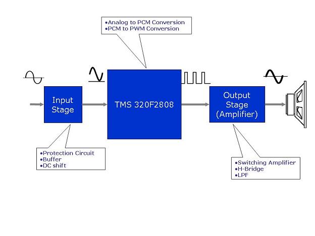
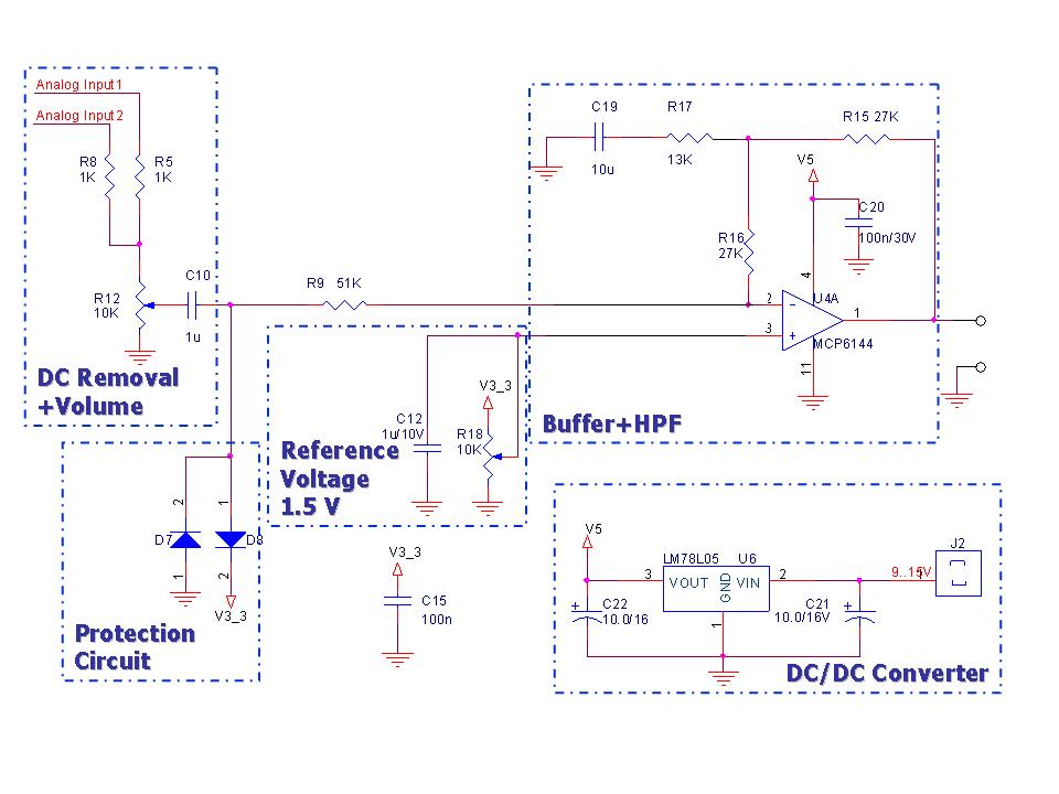
This block interfaces with the audio source, attenuates it DC component and limits the input voltage to the ADC to the range 0 - 3.3V. The circuit contains also a DC-DC converter, for the DSP input buffer.
The TMS320F2808, converts the analog signal to a pair of PWM signals that feed the output stage (Please refer to section ). It operates with 100 MHz. The ADC samples the input signal at a 97.656.25 Ksps rate. The ePWM, generates PWM signal with a period of 102.4 μs and duty cycle proportional to the input signal level. The ePWM coupled with a D-Class output stage and a second order passive RLC filter, provides a DAC equivalent.
The analog signal is converted to PCM values as shown in . The conversion is performed as described in Table 1. The ADC operates in a sampling rate of 97.656 KHz (100 MHz/1024).
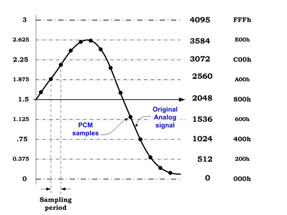
Table 1: Analog to Digital Conversion
| Input Voltage (Vin) | Digital Value(ADCRESULT) |
| 0 | |
| , | |
| 4095 |
The PCM values are converted to PWM as shown in Figure 4. A period of 102.4 msecs (1024 clock cycles) was chosen. The relation PCM Value/Full Range is translated to the duty cycle of the PWM. A duty cycle of 512 (50 %) corresponds to 50% of the full range, for example. In this example sample values in the range 0-4095 will be mapped to duty cycle values (CMPA) in the range 0-1023, by dividing by 4 (shift right 2 bits), as shown in Figure 5.
Notification Switch
Would you like to follow the 'From matlab and simulink to real-time with ti dsp's' conversation and receive update notifications?

|
|

|
|
|
|
|

|
|

|
|

|
|

|
|
|
|
|

|
|

|