

| << Chapter < Page | Chapter >> Page > |
SSPD_Chapter 7_Part 6_Basic Circuit Concepts_continued 4
7.6.5. Driving off-chip capacitive loads.
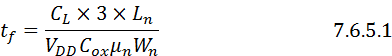
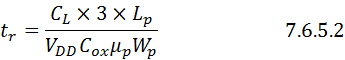
We saw in Section 7.6.4 that transient response is:
Off-chip capacitances are several orders of magnitude greater than the standard gate-to-channel capacitance □C g .
Typically off-chip capacitance C L ≥ □C g . To minimize the charging and discharging delays of the off-chip capacitance we must minimize the pull-up and pull-down channel resistance which can be done by making the channel width W>>the channel L. But this will mean large (W×L) area of the gate of the driver CMOS and this will also cause very large input capacitance of the driver CMOS. The large input capacitance of the driver CMOS will again cause a inordinate delay in the system. So an alternative has to be adopted.
7.6.5.1.Cascaded CMOS Inverters as Drivers.
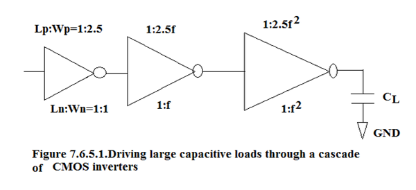
To optimize the drive of off-chip capacitances we must use cascade of CMOS inverters as shown in Figure 7.6.5.1.
We have seen that CMOS inverter driven by another inverter has best performance when Wp =2.5Wn. The proceeding inverters maintain the same pull-up to pull-down resistance ratio but the width is widened by a factor f.
So if first stage has width =Wn =2λ then the second stage has Wn = 2λ×f and third stage has Wn = 2λ×f×f.
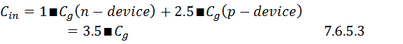
For minimum size lambda based geometries this results in an input capacitance:
This optimized CMOS has symmetric switching transients hence :
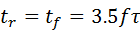
Therefore total delay per CMOS pair is 7fτ where τ is the standard delay unit as described in Section 7.6.3.
We have to optimize the cascaded configuration so as to minimize the number of stages for a given off-chip capacitance C L .
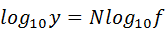
Let us define a capacitance ratio y as:
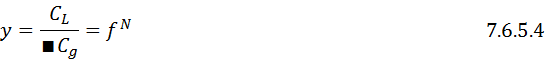
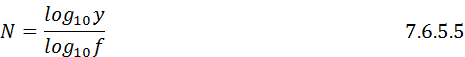
N = number of cascade stages. For a given y we have to arrive at the minimum value of N for a given y.
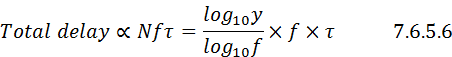
Therefore
The overall total delay in case of CMOS is
= Nt r =Nt f =(N/2)(t r +t f )=3.5Nfτ.
By similar consideration total delay in case of NMOS is
=2.5Nfτ.
So in all cases:
If we tabulate the results of Eq 7.6.5.6 we get Table 7.6.5.1.
Table 7.6.5.1. Tabulation of total delay for various values of f(width multiplication factor) for y=10 4
| Log 10 y | f | Total delay in nsec= K×(logy/logf)×f×τ where τ=0.1nsec |
| 4 | 1.5 | K×0.512 nsec |
| 4 | 2 | K×0.4nsec |
| 4 | 2.7 | K×0.377nsec |
| 4 | 3 | K×0.3784nsec |
| 4 | 4 | K×0.4nsec |
So from the Table 7.6.5.1 it is clear that the total delay curve has a minima at f=2.7. Practically we have a soft minima at f=2.7 so we may choose f=3.
In this case from Eq.7.6.5.5, N=logy/logf =8.38 ≈ 8.
So Equation 7.6.5.5 will be used for determining the optimum cascade stage assuming that the width multiplication factor will be 3.
For a positive step input of V DD :
The overall delay for N even: t d =2.5eNτ (NMOS)
t d =3.5eNτ (CMOS)
The overall delay for N odd: t d =[2.5(N-1)+1]eτ (NMOS)
t d =[3.5(N-1)+2]eτ (CMOS)
For a negative step input of V DD :
The overall delay for N even: t d =2.5eNτ (NMOS)
t d =3.5eNτ (CMOS)
The overall delay for N odd: t d =[2.5(N-1)+4]eτ (NMOS)
t d =[3.5(N-1)+5]eτ (CMOS)
In the above equations, ‘e’ is the base of the natural log and has a value 2.7
Notification Switch
Would you like to follow the 'Solid state physics and devices-the harbinger of third wave of civilization' conversation and receive update notifications?

|
|

|
|

|
|

|
|

|
|
|
|

|
|

|
|

|
|

|