| << Chapter < Page | Chapter >> Page > |
SSPD_Chapter 7_Part 5_Stick Diagram of CMOS Logic Gates_continued 3
7.5.2. Stick Diagrams of CMOS Logic Gates.
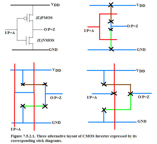
In Figure 7.5.2.1 gives three alternative layouts of CMOS Inverter expressed by its corresponding stick diagram.

Blue colour- metal1, Red – Poly-Si, Green – N+ diffusion, Brown – P+ duffusion, Black Cross is CONTACT.
7.5.3. CMOS Two-input NAND Gate
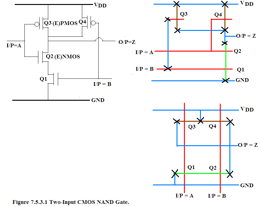
Figure 7.5.3.1 gives the circuit diagram and its alternative layout expressed in stick diagrams for a two-input NAND Gate.. Output Z = Complement(AB)
This means when A=1 and B=1 output is connected to GND bus by a low reesistance through Q1(ON) and Q2(ON) in series. When either of the two I/Ps is at ‘0’ low resistance path to GND is broken and a low reesistance path exists through Q3 or Q4 to 5V(Vdd) bus. Thus the condition for Output Z = Complement(AB) is satisfied.

In Figure 7.5.3.1, Q3 input is shorted to Q1 input and Q4 input is shorted to Q2. In the upper stick diagram, Q4 input and Q2 inpt are connected by the same Red Poly-Si line. But Q3 and Q1 input cannot be connected in the same way. If Q3 and Q1 inputs were connected by the same red line then it would short to the input of Q2 also which it should not. Therefore a metal line blue line is used to cross the red input of Q2. Metal blue line lies at an upper layer while red Poly-Si line lies at intermediate level therefore cross-over is permitted. Once the cross-over has taken place then the two terminals of blue metal line is connected to the two Poly-Si red inputs of Q3 and Q1.
Similarly 3-input NAND Gate can be designed. In case of 3-input NAND Gate we have Q1,Q2 and Q3 in series and Q4,Q5 and Q6 in parallel.
Q1 and Q4 are paired as CMOS, Q2 ans Q5 are paired as CMOS and Q3 and Q6 are paired as CMOS.

Notification Switch
Would you like to follow the 'Solid state physics and devices-the harbinger of third wave of civilization' conversation and receive update notifications?