<< Chapter < Page Chapter >> Page >
SSPD_Chapter 7_Part 4_CMOS Layout conclusion gives the design rules for contact enclosures, device well to device well spacing and the complete N-Well CMOS layout with the PMOS:NMOS =(W/L)p:(W/L)n = 2:1 for best noise margin.

SSPD_Chapter 7_Part 4_CMOS design rules_continued3

7.4.3.1. Device Well-Device Well spacing should be 3Lambda.

7.4.4. Metal Overlay on Diffusion Contact/Poly Si Contact/Metal 1,Metal 2 Via.

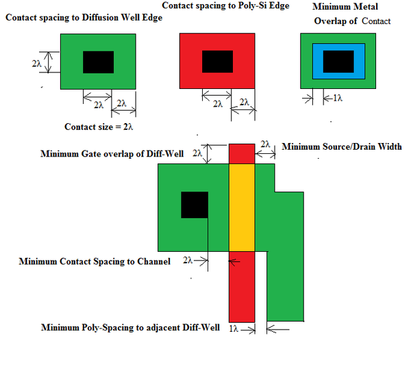
In Figure 7.4.4.1 we give the design rules for Contact Size and Contact Spacing with respect to Diffusion Well/PolySi Edge /Channel, minimum poly-spacing with respect to adjacent diffusion well, minimum gate overlap of Diffusion –Well and minimum Source/Drain width according to CUMF NMOS Design Rules. Contact area is marked black.

Figure 7.4.4.1. The design rules for Contact Size and Contact Spacing with respect to Diffusion Well/PolySi Edge /Channel, minimum poly-spacing with respect to adjacent diffusion well, minimum gate overlap of Diffusion –Well and minimum Source/Drain width according to CUMF NMOS Design Rules. Contact area is marked black.

In Figure 7.4.4.2 we give the definition of Via and how through Vias different level of metallization are interconnected. Minimum distance between two vias is 3Lambda.

7.4.5. Rules for CMOS Layout.

CMOS can be fabricated by the following three methods:

  1. N-Well in P-Substrate;
  2. P-Well in N-Substrate;
  3. Twin Well in P-Substrate.

We will choose N-Well in P-Substrate. In this case we have the following three requirements:

1. Definition of n-well area

2. Threshold implant of two types of transistor

3. Definition of source and drains regions for the NMOS and PMOS.

To ensure the separation of the PMOS and NMOS devices, n-well supporting PMOS is 6lambda away from the active area of NMOS transistor.

This is to prevent overlap of the associated regions as shown in Figure 7.4.5.1.

Simplest MOS processes require only 4 masks. It can be p-channel or n-channel FETs, not both.

In CMOS we have n and p transistors transistors simultaneously and therefore CMOS is a major improvement over NMOS or PMOS technology.

7.4.5.1. Complete CMOS Layout.

We have seen that for maximum noise margin, CMOS should have symmetrical operation around Vin = Vout = 0.5 V DD . This requires that special transconductance parameter β N = β P . Since mobility of majority carriers in PMOS is half that of majority carriers in NMOS hence (W/L) P = 2× (W/L) N . Based on this inference the CMOS layout is given in Figure 7.4.5.2.

Questions & Answers

what is phylogeny
Odigie Reply
evolutionary history and relationship of an organism or group of organisms
AI-Robot
ok
Deng
what is biology
Hajah Reply
the study of living organisms and their interactions with one another and their environments
AI-Robot
cell is the smallest unit of the humanity biologically
Abraham
what is biology
Victoria Reply
what is biology
Abraham
HOW CAN MAN ORGAN FUNCTION
Alfred Reply
the diagram of the digestive system
Assiatu Reply
allimentary cannel
Ogenrwot
How does twins formed
William Reply
They formed in two ways first when one sperm and one egg are splited by mitosis or two sperm and two eggs join together
Oluwatobi
what is genetics
Josephine Reply
Genetics is the study of heredity
Misack
how does twins formed?
Misack
What is manual
Hassan Reply
discuss biological phenomenon and provide pieces of evidence to show that it was responsible for the formation of eukaryotic organelles
Joseph Reply
what is biology
Yousuf Reply
the study of living organisms and their interactions with one another and their environment.
Wine
discuss the biological phenomenon and provide pieces of evidence to show that it was responsible for the formation of eukaryotic organelles in an essay form
Joseph Reply
what is the blood cells
Shaker Reply
list any five characteristics of the blood cells
Shaker
lack electricity and its more savely than electronic microscope because its naturally by using of light
Abdullahi Reply
advantage of electronic microscope is easily and clearly while disadvantage is dangerous because its electronic. advantage of light microscope is savely and naturally by sun while disadvantage is not easily,means its not sharp and not clear
Abdullahi
cell theory state that every organisms composed of one or more cell,cell is the basic unit of life
Abdullahi
is like gone fail us
DENG
cells is the basic structure and functions of all living things
Ramadan
What is classification
ISCONT Reply
is organisms that are similar into groups called tara
Yamosa
in what situation (s) would be the use of a scanning electron microscope be ideal and why?
Kenna Reply
A scanning electron microscope (SEM) is ideal for situations requiring high-resolution imaging of surfaces. It is commonly used in materials science, biology, and geology to examine the topography and composition of samples at a nanoscale level. SEM is particularly useful for studying fine details,
Hilary
Got questions? Join the online conversation and get instant answers!
Jobilize.com Reply

Get Jobilize Job Search Mobile App in your pocket Now!

Get it on Google Play Download on the App Store Now


Source:  OpenStax, Solid state physics and devices-the harbinger of third wave of civilization. OpenStax CNX. Sep 15, 2014 Download for free at http://legacy.cnx.org/content/col11170/1.89
Google Play and the Google Play logo are trademarks of Google Inc.

Notification Switch

Would you like to follow the 'Solid state physics and devices-the harbinger of third wave of civilization' conversation and receive update notifications?

Ask