<< Chapter < Page Chapter >> Page >
SSPD_Chapter 6_ Part 6 introduces us to CMOS process flow upto to the fabrication of P-tub and N-tub.

SSPD_Chapter 6_Part 6_ MOS ICs Fabrication Technology

Because of the inherent advantage of MOS ICs, today MOS Technology dominates the IC market as compared to Bipolar Technology. Table 6.10 gives a comparative study of the two technologies.

Table 6.10 Comparative study of Bipolar and MOS Technologies.

Bipolar Technology MOS Technology
Carrier participation in transistor action Both majority and minority carriers partake in transistor action-bipolar Only majority carriers partake in transistor action-unipolar
speed Traditionally much faster Slower devices
Power dissipation Higher dissipation CMOS is nano watt logic under standby condition
Packing density One generation behind because of isolation diffusion Much higher packing density
Design flexibility Higher design flexibility
Noise Figure Higher noise figure Quieter devices.
Dynamic range Input dynamic range is 5mV because it is exponential device. Input dynamic range is 400mV because it is a quadratic device.

Semiconductor Industry Association(SIA) brought out the National Technology Roadmap for Semiconductors(NTRS) in 1994, updated in 1997 , again in 1999 and again in 2001. Based on that data we give the following Table 6.11.

Table 6.11. Future Projections for Silicon Technology taken from SIA NTRS (1997).

Year of the first DRAM shipment 1997 1999 2003 2006 2009 2012
Minimum feature size(nm) 250 180 130 100 70 50
Memory size(bits/chip) 256M 1G 4G 16G 64G 256G
DRAM Chip size(mm 2 ) 280 400 560 790 1120 1580
µP transistors/chip 11M 21M 76M 200M 520M 1.4B
Maximum wiring levels 6 6-7 7 7-8 8-9 9
Minimum mask count 22 22-24 24 24-26 26-28 28
Minimum supply voltage 1.8-2.5 1.5-1.8 1.2-1.5 0.9-1.2 0.6-0.9 0.5-0.6

Table 6.12 Updating of 1997 SIA NTRS Roadmap in 1999 and 2001.

2004 2005 2007 2008 2010 2011 2013 2014 2016
1999_NTRS 100nm 70nm 50nm 35nm
2001_NTRS 90nm 65nm 45nm 32nm 22nm

By a variety of post-lithographic techniques, the physical gate length is shorter than the printed size in photo-resist. It is projected to be 9 nm by 2016. "Lithography half-pitch and transistor gate length scaling trends continue to accelerate. This means that semiconductor chips will continue to get smaller, faster and ultimately less expensive at an even faster rate in the future," noted Paolo Gargini, Chairman of the International Roadmap Committee and Fellow, Intel Corporation "When the 2001 Roadmap looks 15 years into the future, the physical gate length is projected to be a mere 9 nanometers. We are beginning to consider technologies beyond planar or even post-CMOS devices."

In 1970, NMOS IC Technology was introduced but it was replaced by CMOS IC Technology by 1980. So our discussion will concentrate on CMOS Process Flow.

Section 6.6.1. NMOS IC in 1970s.

For academic reasons, we introduce the cross-section view of NMOS IC in Figure 6.39. This was prevalent in 1970s. This includes both enhancement type NMOS and depletion type NMOS.

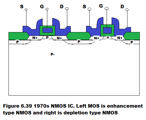
In Figure 6.39, blue colour represents METAL CONTACT and green colour represents OXIDE. Thin oxide is gate oxide and thick oxide is field oxide.

Questions & Answers

what does preconceived mean
sammie Reply
physiological Psychology
Nwosu Reply
How can I develope my cognitive domain
Amanyire Reply
why is communication effective
Dakolo Reply
Communication is effective because it allows individuals to share ideas, thoughts, and information with others.
effective communication can lead to improved outcomes in various settings, including personal relationships, business environments, and educational settings. By communicating effectively, individuals can negotiate effectively, solve problems collaboratively, and work towards common goals.
it starts up serve and return practice/assessments.it helps find voice talking therapy also assessments through relaxed conversation.
miss
Every time someone flushes a toilet in the apartment building, the person begins to jumb back automatically after hearing the flush, before the water temperature changes. Identify the types of learning, if it is classical conditioning identify the NS, UCS, CS and CR. If it is operant conditioning, identify the type of consequence positive reinforcement, negative reinforcement or punishment
Wekolamo Reply
please i need answer
Wekolamo
because it helps many people around the world to understand how to interact with other people and understand them well, for example at work (job).
Manix Reply
Agreed 👍 There are many parts of our brains and behaviors, we really need to get to know. Blessings for everyone and happy Sunday!
ARC
A child is a member of community not society elucidate ?
JESSY Reply
Isn't practices worldwide, be it psychology, be it science. isn't much just a false belief of control over something the mind cannot truly comprehend?
Simon Reply
compare and contrast skinner's perspective on personality development on freud
namakula Reply
Skinner skipped the whole unconscious phenomenon and rather emphasized on classical conditioning
war
explain how nature and nurture affect the development and later the productivity of an individual.
Amesalu Reply
nature is an hereditary factor while nurture is an environmental factor which constitute an individual personality. so if an individual's parent has a deviant behavior and was also brought up in an deviant environment, observation of the behavior and the inborn trait we make the individual deviant.
Samuel
I am taking this course because I am hoping that I could somehow learn more about my chosen field of interest and due to the fact that being a PsyD really ignites my passion as an individual the more I hope to learn about developing and literally explore the complexity of my critical thinking skills
Zyryn Reply
good👍
Jonathan
and having a good philosophy of the world is like a sandwich and a peanut butter 👍
Jonathan
generally amnesi how long yrs memory loss
Kelu Reply
interpersonal relationships
Abdulfatai Reply
What would be the best educational aid(s) for gifted kids/savants?
Heidi Reply
treat them normal, if they want help then give them. that will make everyone happy
Saurabh
What are the treatment for autism?
Magret Reply
hello. autism is a umbrella term. autistic kids have different disorder overlapping. for example. a kid may show symptoms of ADHD and also learning disabilities. before treatment please make sure the kid doesn't have physical disabilities like hearing..vision..speech problem. sometimes these
Jharna
continue.. sometimes due to these physical problems..the diagnosis may be misdiagnosed. treatment for autism. well it depends on the severity. since autistic kids have problems in communicating and adopting to the environment.. it's best to expose the child in situations where the child
Jharna
child interact with other kids under doc supervision. play therapy. speech therapy. Engaging in different activities that activate most parts of the brain.. like drawing..painting. matching color board game. string and beads game. the more you interact with the child the more effective
Jharna
results you'll get.. please consult a therapist to know what suits best on your child. and last as a parent. I know sometimes it's overwhelming to guide a special kid. but trust the process and be strong and patient as a parent.
Jharna
Got questions? Join the online conversation and get instant answers!
Jobilize.com Reply

Get Jobilize Job Search Mobile App in your pocket Now!

Get it on Google Play Download on the App Store Now


Source:  OpenStax, Solid state physics and devices-the harbinger of third wave of civilization. OpenStax CNX. Sep 15, 2014 Download for free at http://legacy.cnx.org/content/col11170/1.89
Google Play and the Google Play logo are trademarks of Google Inc.

Notification Switch

Would you like to follow the 'Solid state physics and devices-the harbinger of third wave of civilization' conversation and receive update notifications?

Ask