

| << Chapter < Page | Chapter >> Page > |
1970s saw the emergence of NMOS technology and NMOS based Dynamic Random Access Memory. IBM and Intel provided the technology and MOSTEK gave the Clock Design. This led to the successful marketing of the first VLSI 16K-bit DRAM. Scaling was applied to this DRAM structure.
A consortium of five top Japanese microelectronics companies: Hitachi, NEC, Fujitsu, Mitsubishi and Toshiba worked on VLSI Technology Project and created the complete infrastructure for 256K-bit DRAM . For this they developed Ultra-Clean Rooms in which they ushered in 1-micron VLSI era by the end of 1970s.
By 1980s NMOS circuits were replaced by CMOS due to ease of circuit design. Quasi constant voltage scaling was adopted. Voltage tolerant device structures like the lightly doped drain (LDD) transistor, silicide clad source drain, and hot electron defense was adopted. These technologies provided some of the keys to continue scaling feature sizes slower than voltage . 1980s saw the crossing of 1 micron barrier and formally we entered into sub-micron technology era.
In 1980s only Carver Meade and Lynn Conway wrote a book by the title “Introduction to VLSI System”. In this they simplified the design rules of CMOS circuit by introducing Linear Device Scaling Theory. University of California, Berkeley, introduced ‘CADENCE’- a suite of design tools of CMOS circuits. This connected the device physics to logic circuits, logic circuits to circuit design and verification tools to check the design rules. The entire ASIC world of semi-custom chips opened up based on this set of abstractions and made scaling applicable to all chips.
In 1990, Stanford developed process simulators and device simulators. They incorporated the scaling in Generation of Process Technology and a given Generation could be used for implementing a given system. Complex Systems would be implemented by advanced Generations. Thus emerged Technology Computer-Aided-Design today popularly known as TCAD.
In order to make TCAD commercially viable, manufacturing yield and defect analysis had to be included. Redundancy and repair techniques were included. Yield analysis tool (developed at Carnegie Mellon University), defect measurement tools, systematic yield process and ramp process kept ‘linear scaling’ commercially viable. This enabled scaling beyond 256K-bitDRAM.
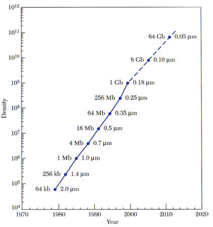
Figure 6.29. Scaling of Memory Chips.
As seen in Figure 6.29, from late 1970 the 2µm Generation of Technology(64kb per chip) improved to 0.18µm Technology (1Gb per chip) in 2000 for memory chips. In the same period Generation of Technology for logic chips improved from 10K devices to 100M device-count per chip as shown in Figure 6.30. As is evident from the two figures, Memory-Chip has been full one Generation ahead of Logic-Chips as far as technology is concerned.
Because of the edge of Japan over USA in early 80s in sub-micron VLSI Memory chips, USA under the aegies of Defence Advanced Research Program Agency (DARPA) started Microelectronics Manufacturing Science&Technology (MMST) Program. DARPA made a consortium with Texas Instruments, US Air-Force, Semi-conductor Equipment manufacturers and University Researchers. Its purpose was the following:
Notification Switch
Would you like to follow the 'Solid state physics and devices-the harbinger of third wave of civilization' conversation and receive update notifications?

|
|

|
|

|
|

|
|

|
|

|
|

|
|
|
|
|
|
|
|
|
|