

| << Chapter < Page | Chapter >> Page > |
Initially the growth rate over a fresh silicon surface is reaction controlled since for thin layer the growth is decided by the reaction rate of reacting Si and O 2 .
In Reaction Controlled Oxidation
x =

B/A = linear rate constant.
Where A, B and T are constants
X= thickness of oxide, t = time of oxidation.
Definition of thin layer is: X<<A/2

When oxide layer is thick i.e. X>>A/2 (long duration oxidation)
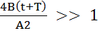

Here the rate is parabolic and B = parabolic constant .
Because of initial linear law of growth and finally parabolic law of growth during oxidation over a silicon surface with an initial oxide step , the step gets invisible and after long oxidation duration we get a smooth plane surface as shown in the Figure (6.6).
This is very desirable feature for I.C fabrication because metallic inter connection are over the oxide surface covering the chip . The removal of undulations by long duration oxidation makes metallic interconnection reliable and of uniform strengths .
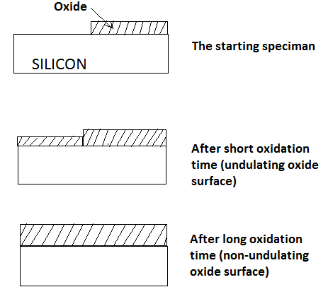
Figure 6.6. Over the total fabrication cycle the linear and parabolic law compensate each other to provide a planar oxide surface which is ideal for depositing Al layer and etching out the interconnections.
By putting the wafer in oxidation furnace we get an uniformly thick oxide layer.
Typical furnace cycle is 15 minutes at 900°C in an H 2 O ambient. This produces 40nm thick oxide layer. The usual practice is to make H 2 and O 2 react in the back end of the furnace to produce steam for H 2 O ambient. This is a cleaner method for producing steam.
This same 40nm could be achieved by a furnace cycle of 45 minutes at 1000°C in dry oxidation ambient
Bruce Deal and Andy Grove developed linear-parabolic model for thermal oxidation. This is referred to as Deal-Grove model. It is used in SUPREM software developed by Stanford for process simulation.
Often we need a local thick oxide layer as is the case in CMOS technology. This thick local oxide layer is called field oxide and it helps electrically isolate two adjacent MOS devices. This thick local oxide layer is achieved by a technique called LOCOS (LOCal Oxidation of Silicon).
6.4.3 .Technology of LOCOS
As shown in Figure (6.7), 40 nm thick Oxide Layer is grown in Oxidation furnace and in a second furnace 80 nm thick Silicon Nitride layer is grown by Low Pressure Chemical Vapour Deposition (LPCVD) method.
4NH 3 + SiH 4 = Si 3 N 4 ↓ + 12H 2 ↑
This reaction is carried out at 800ºC below atmospheric pressure. This helps a better uniformity of deposited films over large lots of wafers.
Si3N4 is covered by KPR and exposed through a suitable mask. We use positive KPR so that exposed portion remains soft and it is dissolved by the developer. The portion where local oxidation is to take place there KPR is dissolved and the portion where no local oxidation is required there the KPR is retained and fixed. Through the aperture in KPR film, dry etching of Si3N4 is carried out in Fluorine Plasma Chamber. As the feature size has decreased due to lateral and vertical scaling we have moved from WET PROCESSING to DRY PROCESSING.
Notification Switch
Would you like to follow the 'Solid state physics and devices-the harbinger of third wave of civilization' conversation and receive update notifications?

|
|

|
|

|
|
|
|
|
|
|

|
|

|
|

|
|

|
|
|
|