

| << Chapter < Page | Chapter >> Page > |
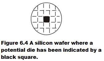
The resistivity of the p type substrate is kept very high (10 ohm-cm) because all the components on a single chip will be isolated from one another by being kept reverse biased with respect to the substrate . Since substrate is p type it will be kept at most negative potential “-V EE “. And the most positive potential of the circuit is “V CC ”. Therefore maximum reverse potential with respect to substrate will be (V CC +V EE ). Hence substrate breakdown voltage must be high and at the same time the parasitic coupling of each component to the substrate must be kept at a minimum so as to derive optimum high frequency performance out of the chip. Both these objectives are achieved by having high resistivity.
6.4.2 . Thermal oxidation :
Next important fabrication step is thermal oxidation which enables the growth of a uniform thin skin of SiO 2 , approximately 3,000A o to 10,000A o thick (0.3 to 1 µm), over the clean silicon surface.
3000×10 -10 m=0.3×10 -6 m= 0.3um(micro meter) = 300nm.
Silicon dioxide plays four important roles in I.C. fabrication namely acts as i. mask for diffusion, as ii.Gate Oxide in MOSFET, as iii. Field Oxide for electrically isolating the MOSFETs and for iv. passivation.
At 45nm technology, the mask is typically 100nm thick, Gate Oxide is 40nm thick, field Oxide is 200nm thick and passivation layer is 300nm thick.
SiO 2 layer for Masked diffusion or ion implantation – Most of the dopants or impurities commonly used for doping have very low diffusion coefficients in SiO 2 as a result even a long exposure to dopant (or impurity) atoms at high temperature no impurities penetrate SiO 2 . This property enables one to etch apertures of selected shape and size in SiO 2 layer by the use of photolithographic techniques and then the wafer is exposed to the diffusion at given temperatures for given time. Because of masking property of SiO 2 only selective diffusion through the aperture into Si wafer takes place. Thus by masked diffusion , using SiO 2 mask suitably, the conductivity properties of the wafer are modified in desired localized region in a controlled fashion.
P type dopants (group III elements ) are boron(B), Aluminium (Al),gallium(Ga). Boron has very slow diffusion in SiO 2 but rapid diffusion is Si whereas Gallium has rapid diffusion in both. On the other hand Aluminum has very low solid solubility in Si (maximum surface concentration is only 0.002 percent) therefore Al used only for ohmic contact pads. Hence in masked diffusion, Boron is universally used as P type diffusant .
N type dopants are Phosphorous (P) and Arsenic (As). Both are effectively masked by SiO 2 but ‘As’ has very low diffusion constant in Si. Therefore Phosphorous is universally used as N type diffusant . B and P have nearly equal diffusion constants in Si and they both have very high solid solubility, permitting a high surface concentration.
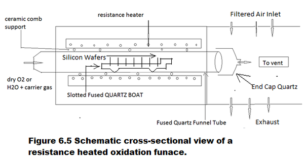
[ The silicon wafer loading area is always in the laminar hood. The laminar flow hood reduces dust and particulate matter in the air surrounding the wafers and minimizes contamination during wafer loading]
Notification Switch
Would you like to follow the 'Solid state physics and devices-the harbinger of third wave of civilization' conversation and receive update notifications?


