

| << Chapter < Page | Chapter >> Page > |
Chapter 4. Section 4.2. Structure of IC NPN BJT.
In Figure 4.2.1. the Cross-sectional view of Integrated Circuit Vertical NPN Transistor is shown.
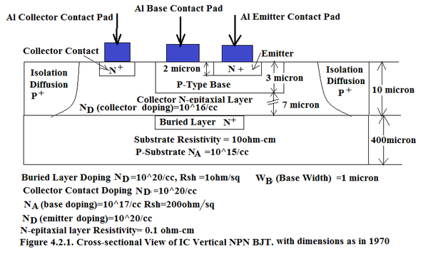
In 1960, we had micron scale BJT with Base Width(W B ) = 1μm. Today in 2013 we have nano-scale BJT with Base Width= 10nm. In last 50 years with the advancement of IC Technology we have scaled down the Base Width by 1/100 times. This has resulted in improvement of Transit Frequency f T from 100MHz to 500GHz. This is 5000 times improvement in speed.
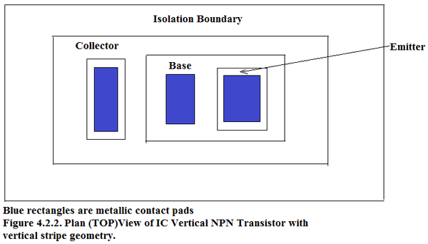
Figure 4.2.2. gives the top view of Vertical NPN Transistor. As seen in Figure 4.2.1. There is 400 micron thick wafer of 300mm diameter. Now we are moving to 450mm diameter wafer for IC fabrication. This is called the substrate and it provides the mechanical strength to the IC fabricated over it. Where ever vertical NPN transistor is situated underneath it 1 micron deep Buried Layer is provided to give a very low resistance path to the collector current. If Buried Layer is not there then collector bulk series resistance will become high leading to large Vsat voltages.
In saturation mode, transistor operates in cut-off mode and saturation mode. In Cut-off Mode transistor gives 5V output which corresponds to ‘1’ bit. In Saturation Mode transistor output is 0.2V and this corresponds to ‘0’ bit. If buried layer is not introduced then there will be considerable drop across series resistance of Collector bulk leading to Vsat = more than 1V. This is not a realistic ‘0’ bit. Hence buried layer is essential in case of Logic Applications.
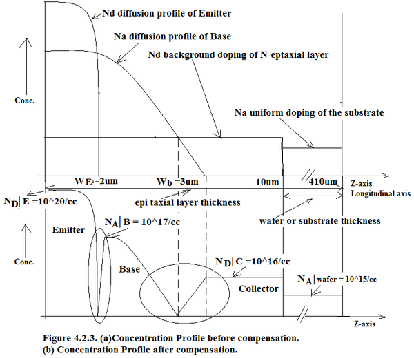
In Figure 4.2.3. the concentration profile before and after compensation is shown for IC Vertical NPN Transistor. The substrate is a wafer of 400μm thickness and has uniform doping of 10 15 per cc which corresponds to a ρ = 10 Ω-cm. Over the substrate a 10μm thick N-Type epitaxial layer is grown with a background doping of 10 16 per cc which corresponds to 0.1 Ω-cm. The actual IC components are fabricated in the epitaxial layer. The substrate is only for providing mechanical strength to the IC. Metallic interconnections (of Al or Cu) are made on the top surface of the epitaxial layer. Hence it is called Planar Technology.
Base diffusion is a long drive-in for several hours from a limited source up to more than 3μm depth. Hence Base Diffusion Profile is a Gaussian Profile.
Emitter Diffusion is a short diffusion from infinite source. Hence Emitter Diffusion is a complementary error function.
After compensation we obtain an Abrupt Junction at EB metallurgical junction and we obtain linearly-graded junction at BC metallurgical junction.
Emitter is heavily N-type doped at 10 20 /cc. This is equivalent to Sheet Resistance R Sheet =1Ω/square. In contrast Base is linearly graded from 10 17 /cc on Emitter side to 0 /cc on Collector side. This corresponds to R Sheet = 200Ω/cc. This large differential in sheet resistance helps achieve Emitter Injection Efficiency of nearly 100%. The linearly graded impurity profile creates an in-built electric field which aids the diffusion of minority carriers across the Base Junction as we will see in the Design Rules.
17
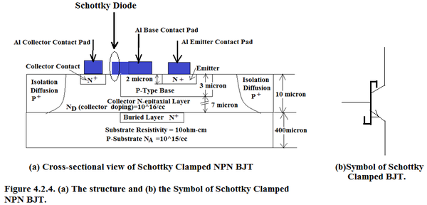
In Figure 4.2.4. we show the structure of Schottky Clamped NPN Transistor. As shown in the Figure 4.2.4. the Base Metallic Contact is extended upto collector. Metal-N-Type Semiconductor Interface becomes a Schottky Diode.
This modification greatly reduces the switching time of TTL gates. Without Schottky Diodes, when “1” bit is impressed on the Base of a RTL Inverter, the base current drives the Gate Transistor is into ‘DEEP SATURATION’. But in case of Schottky Clamped transistor, even before BC Junction is forward biased, Schottky diode turns ON and shunts the base current as a result Gate Transistor is driven into Shallow Saturation and minority carrier build-up in Base is limited. Hence Transistor easily switches off. This results into much faster switching of Schottky Clamped TTL gates.
Notification Switch
Would you like to follow the 'Solid state physics and devices-the harbinger of third wave of civilization' conversation and receive update notifications?

|
|

|
|

|
|

|
|

|
|

|
|
|
|

|
|

|
|

|