

| << Chapter < Page | Chapter >> Page > |
Tutorial Sheet of Chapter 3.Diode Physics.
Question 1 . Pspice is a software which is used for Circuit and System Simulation. The Diode adopted in it, if not specified, has the following fabrication parameters and geometrical dimensions:
| P-doping | 10 16 /cc | N-doping | 5×10 15 /cc | comments |
|---|---|---|---|---|
| Abrupt Junction | m= 1/2 | NA | NA | C j varies as 1/√(Φ BO +V R ) |
| W P | 5μm | W N | 5μm | Bulk Width on two sides |
| Cross-SectionalArea | NA | NA | NA | 100μm×100μm |
| Diffusion Coeff. | D P =10cm 2 /s | NA | D N =30cm 2 /s | NA |
| Life Time | τ P =0.1μs | NA | τ N =0.1μs | τ(depletion)=0.1μs |
| Mobility | 384cm 2 /(V-s) | NA | 1153cm 2 /(V-s) | NA |
| Diffusion Length | 0.001cm=10μm | 0.001732cm=17.32μm | L 2 =Dτ |
NA-not applicable.
i.The current density should not exceed 10 3 A/cm 2 .If the current density exceeds this value it is going to disrupt Aluminum interconnections. Nowadays with the scaling reaching its limit, the above current density is being exceeded leading to the failure of the devices. Hence Al interconnection is being superseded by Cu interconnection.
Hence if the maximum rated current is 100mA then the cross-sectional area should be 100μm×100μm.
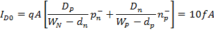
ii.Since Diffusion Length is longer than Bulk width hence it is Narrow Bulk Diode.
iii.The total depletion width =
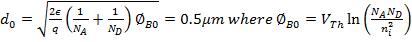

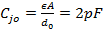
iv.Junction Capacitance=
v. Reverse Saturation Current=Reverse Leakage Current for Narrow Bulk Diode=
vi. Reverse Leakage Current for a Wide Bulk Diode (when Bulk Width is 10 times the diffusion length then we fulfill the criteria for Wide Bulk Diode)=
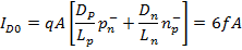
As we see the leakage current in Narrow Bulk Diode is larger than that in Wide Bulk Diode which is not desirable but its switching transients are much better as the minority carrier stored can be reduced considerably by reducing the bulk width.
vii. The Calculation of Avalanche Break-Down Voltage=BV A :
At the Avalanche breakdown point, E max at the metallurgical junction is equal to E critical = 5×10 5 V/cm and let the depletion width be d* then from the first principles:
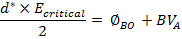
Solving this equation we get: √(Φ BO +BV A ) = 15.2989
Therefore: (Φ BO +BV A ) = 234.05
Therefore BV A = 233.37V.
Calculate : i. Reverse Saturation Current [Answer 10 -14 A=10fA]
ii.Junction Capacitance at zero bias [Answer 2pF]
iii.Built-in barrier Potential [Answer 0.68V]
iv.BV A ( Avalanche Breakdown Voltage) [Answer 233V]
Once the design is complete the fabrication parameters, the method of diffusion and geometrical dimensions are sent to the Solid State foundry where the given Diode is fabricated and sent back to the customer for testing the design parameters.
Question 2 . For an abrupt junction diode, N A =10 17 /cc and N D =10 16 /cc.
ε=10 -10 F/m]
Question 3. Fill up the Table Below:
| N A (per cc) | N D (per cc) | Φ BO (V) | d 0 (μm) |
|---|---|---|---|
| 10 17 /cc | 10 16 /cc | ? | ? |
| 10 19 /cc | 10 16 /cc | ? | ? |
| 2.5×10 16 /cc | 10 16 /cc | ? | ? |
Answer:
| N A (per cc) | N D (per cc) | Φ BO (V) | d 0 (μm) |
|---|---|---|---|
| 10 17 /cc | 10 16 /cc | 0.778 | 0.327 |
| 10 19 /cc | 10 16 /cc | 0.898 | 0.335 |
| 2.5×10 16 /cc | 10 16 /cc | 0.682 | 0.345 |
Question 3. Determine E max and d no and d po in Problem 2?
[E max =47.584KV/cm, d po =0.0297μm, d no =0.297μm]
Question 4. If reverse saturation current =40fA then determine I D for V D = 0.7V and V D = 0.55V[Answer 19.7mA, 61.525μA].
If forward diode current = 6mA the determine the applied voltage across the diode?[0.669V]
Assume Ideality factor =1 .
Question 5. If reverse saturation current =5fA then determine I D for V D = - 0.04V and V D =
-2V[Answer -3.92fA, -5fA].
Question 6. When I D =1.14mA what is V D at 300K if I DO =5fA.[Ans.0.68V]
What is the diode voltage at275K and at 350K if Diode Current is to be maintained constant.[0.742V,0.555V]
Diode Forward Voltage V D changes by -2.5mV per Kelvin for maintaining the forward diode current constant.
Question 7. Given η=1,I DO =10fA and Thermal Voltage(V Th ) =25mV. Determine diode current at Diode Voltage=0.7V,0.65V,0.6V,0.4V,-0.1V and -5V.
[Answer:14.46mA,1.95mA,0.26mA,88nA,-9.8fA and -10fA]
Question8. Given η=1,I DO =100fA and Thermal Voltage(V Th ) =25mV. Determine diode current at Diode Voltage=0.4V and determine diode voltage for diode current=1mA.
[0.888μA,0.576V]
Question 9. Given η=1,determine the factor by which current increases if forward diode voltage is increased by 100mV.[Hint:60mV increase gives a decade increase; Answer: factor of 46.4]
Question 10. In a Si Diode 1N4135, I DO (300K)=10nA. Determine I DO (316K). [30.3nA]
Hint: I DO (316K)= I DO (300K)×2 (T-300K)/10K = 10nA×2 (316K-300K)/10K =10nA×2 1.6 =30.3nA.
Question 11. At 300K, forward bias of a diode = 0.7V and forward diode current = 7.42mA. To maintain the current constant at 7.42mA determine V D * at 316K. [660mV]
Question 12. In 1N4135, at 300K the current flowing through the diode is I D = 10mA
given I DO (300K) = 10nA and η=2 . Using the Real Diode Equation, forward diode Voltage is determined to be V D =0.7185V.
If the forward diode current is to be maintained constant at 10mA then determine V D at 290K, 310K and at 320K.
Solution : Using the Real Diode Equation we get:
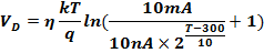
Using the above equation we obtain forward diode voltage at T =290K, 300K, 310K and 320K.
The answers are:
| Temperature(K) | 290 | 300 | 310 | 320 |
|---|---|---|---|---|
| V D (V) | 0.725 | 0.714 | 0.701 | 0.6855 |
Question 13. Given I DO (300K) = 10nA,η = 2. Determine I D at V D = 0.6V and at 0.7V. [Ans. 1.02mA and 7mA]
If I D = 5mA then determine V D at 300K. [Ans. 0.682V]
Question 14. In a given Si-Diode, I DO (300K) = 1nA,η = 2. At 300K, determine I D at V D = 0.7V, 0.1V, 0V, -0.1V and at -0.7V.
[Ans. 0.702mA, 5.8nA, 0A, -0.854nA, -1nA]
Question 15. In a given Si-Diode, I DO (300K) = 1nA,η = 2. At 300K, determine V D
at I D = -0.5nA, 0A, 0.5nA, 50nA and 50μA.
[Ans. -0.036V, 0V, 0.021V,0.204V, 0.563V]
Question 16. (a)Determine built-in barrier potential Φ BO in a Si-diode. Silicon packing density is 5×10 22 atoms/cc. P-Side doping is 1Acceptor Atom per 10 8 of Si Atoms and N-Side doping is 2 Donor Atoms per 10 7 of Si Atoms.
Hint: P-Side doping is 1Acceptor Atom per 10 8 of Si Atoms implies N A = (5×10 22 /10 8 ) /cc = 5×10 14 /cc.
N-Side doping is 2 Donor Atoms per 10 7 of Si Atoms implies N D = (5×10 22 /(10 7 /2) ) /cc=1×10 16 /cc.
[Ans.0.64V]
(b) Determine built-in barrier potential Φ BO in a Si-diode where :
| P-side | N-side | |
|---|---|---|
| σ | 50S/m | 100S/m |
| μ | 0.05m 2 /(V-s) | 0.13m 2 /(V-s) |
Hint:


Therefore Φ BO =0.687V.
Notification Switch
Would you like to follow the 'Solid state physics and devices-the harbinger of third wave of civilization' conversation and receive update notifications?

|
|

|
|

|
|

|
|

|
|

|
|

|
|

|
|

|
|

|