

| << Chapter < Page | Chapter >> Page > |
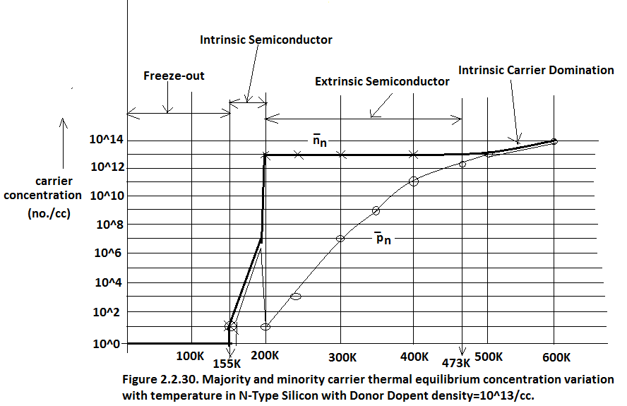
There are four distinct regions of Doped Silicon:
Freeze out region (0K to 155K) - neither there is EHP thermal generation nor there is the ionization of the donor atoms.
Intrinsic Semiconductor (155K to 200K) - thermal generation of EHP starts but there is no ionization of Donor Atoms.
Extrinsic Semiconductor (200K to 473K) – Ionization of Donor atoms is 100% hence majority carriers thermal equilibrium density is decided by Donor Density hence it is constant at 10 13 /cc. Thermal generation of EHP is taking place but it is many orders of magnitude less than the majority carrier hence from 200K to 473K resistivity of the sample is relatively constant.
Intrinsic Carrier Concentration dominates over the doping density(473K and beyond) – at 473K , thermal generation of EHP becomes comparable to doping density. At 600K it becomes one order of magnitude greater than the doping density. So in this region it again behaves as Intrinsic Semiconductor.
2.2.6.2.Theoretical Formulation of Majority Carriers and Minority Carriers.
Because of Pauli-Exclusion Principle, we have a term called Density of States N(E). This essentially means the number of electrons which can be accommodated per unit volume per unit eV in permissible energy states.
In the Appendix of this Chapter I will show that:
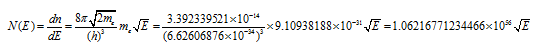
(2.2.6.2.1)
N(E)dE=number of energy states per m 3 between energy level E and E+dE.
Therefore actual number of electrons present in conduction band between energy level E and E+dE are = P(E)N(E)dE
Where P(E) = 1/[1+Exp[(E-E F )/kT];
But at T = 0K, P(E)= 1 upto E = E F hence
actual number of electrons present in conduction band between energy level E and E+dE are = (1)N(E)dE
In Copper we know that electrons are filled up to the Fermi-Level and that the Fermi-level is at 7.05eV as shown in Figure 2.2.31.
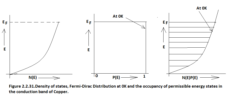
Hence number of conducting electrons in the conduction band from the bottom of the conduction band to Fermi-level=∫(1)K√EdE,{E,0,7.05×1.6×10 -19 }
Here K is a constant = 1.06216771234466×10 56 .
Using Mathematica:

Conduction Band conducting electron density = n= 8.5×10 28 /m 3 =8.5×10 22 /cc.
This also implies that Copper atom packing density in Copper metal is 8.5×10 28 /m 3 =8.5×10 22 /cc.
You can see normally the packing density is of this order i.e.10 22 /cc.
Exactly the same procedure is applied to determine the majority carrier thermal equilibrium density.
In N-Type Silicon:
Number of electrons actually present in the conduction band at 300K=∫P(E)N(E)dE .
This is a definite integral between the lower limit E C and the upper limit infinity as shown below:
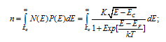
It will be shown in the Appendix of this Section that this integral comes out to be:
Electron density= n n --- = N C Exp[-(E C -E F )/(kT)]_____________(2.2.6.2.4)
Where N C =2[(2πm e *kT)/h 2 ] 3/2 =2.82×10 25 /m 3 = 2.82×10 19 /cc.
Here m e *= effective mass of the electron at the bottom of the conduction band.
For non-degenerate semiconductors where E F is several kT below E C , in such cases
Fermi-Dirac Statistics(P(E) = 1/[1+Exp[(E-E F )/kT]) approximates Boltzmann-Maxwell Statistics namely P(E) = Exp[-(E-E F )/kT].
At E = E C this reduces to P(E C )= Exp[-(E C -E F )/kT].
Hence in Equation 2.2.6.2.4, if Exp[-(E C -E F )/kT] is the probability of occupancy at the lower edge of the conduction band and n n --- is the conduction electron density in conduction band then N C is the effective density of states at E C .
We follow the same procedure for holes concentration calculation:
Number of holes actually present in the valence band at 300K=∫(1-P(E))N(E)dE
This is a definite integral between the lower limit E V and the upper limit (- infinity) as shown below:
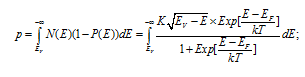
As will be shown in the Appendix this reduces to:
Hole density= p n --- = N V Exp[-(E F -E V )/(kT)] _____________(2.2.6.2.6)
Where N V =2[(2πm h *kT)/h 2 ] 3/2 =1.83×10 25 /m 3 = 1.83×10 19 /cc.
Since Exp[-(E F -E V )/(kT)] = probability of non-occupancy at E V = probability of occurrence of hole at the upper edge of the valenvce band hence N V = is the effective density of states at the upper edge of the valence band.
N V = N C this identity does not hold since the effective masses are not the same as seen in Table 2.2.6.1.
By Law of Mass Action: n n --- × p n --- =n i 2 =N C N V Exp[- E G /(kT)] where E G =E C -E V ;
Hence intrinsic carrier concentration =
n i =√(N C N V ) ×Exp[- E G /(2kT)]_________________________(2.2.6.2.7)
In Table 2.2.5.1. a comparative study of the band-gap, effective mass of electron and hole, effective density of states and intrinsic carrier concentration is made for Ge,Si and GaAs.By the inspection of Table 2.2.5.1, it is evident that density of states are in the range of 10 19 per cc for all three semi-conductors..
Table 2.2.6.1. Band-gap, effective mass , effective densiy of states and intrinsic carrier concentration at 300K.
| All parameters at 300K | Ge | Si | GaAs |
|---|---|---|---|
| E G (eV) | 0.66 | 1.12 | 1.424 |
| (effecteive mass)m e * (×m e ) | 0.56 | 1.08 | 0.067 |
| (effecteive mass)m h * (×m e ) | 0.29 | 0.81 | 0.47 |
| N C (per cc) | 1.05×10 19 | 2.82×10 19 | 4.37×10 17 |
| N V (per cc) | 3.92×10 18 | 1.83×10 19 | 8.68×10 18 |
| n i (per cc) | 1.83×10 13 | 8.81×10 9 | 2.03×10 6 |
Notification Switch
Would you like to follow the 'Solid state physics and devices-the harbinger of third wave of civilization' conversation and receive update notifications?

|
|

|
|

|
|

|
|

|
|

|
|

|
|

|
|

|
|
|
|