

| << Chapter < Page | Chapter >> Page > |
A single crystal of either an elemental (e.g., silicon) or compound (e.g., gallium arsenide) semiconductor forms the basis of almost all semiconductor devices. The ability to control the electronic and opto-electronic properties of these materials is based on an understanding of their structure. In addition, the metals and many of the insulators employed within a microelectronic device are also crystalline.
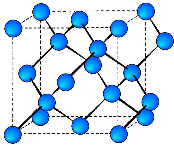
Each of the semiconducting phases of the group IV (14) elements, C (diamond), Si, Ge, and α-Sn, adopt the diamond cubic structure ( [link] ). Their lattice constants ( a , Å) and densities (ρ, g/cm 3 ) are given in [link] .
| Element | Lattice parameter, a (Å) | Density (g/cm 3 ) |
| carbon (diamond) | 3.56683(1) | 3.51525 |
| silicon | 5.4310201(3) | 2.319002 |
| germanium | 5.657906(1) | 5.3234 |
| tin (α-Sn) | 6.4892(1) | 7.285 |
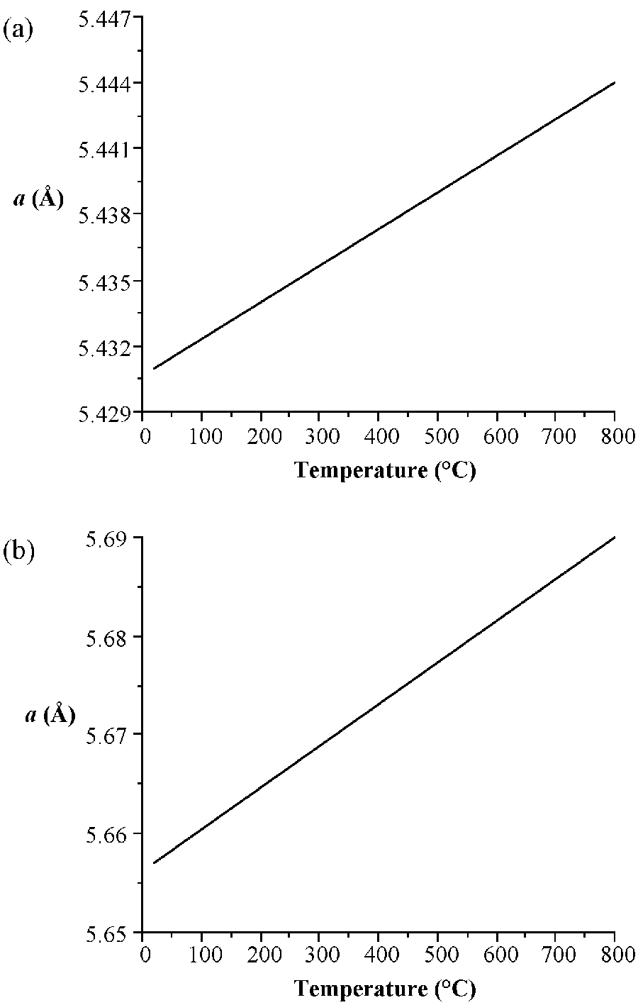
As would be expected the lattice parameter increase in the order C<Si<Ge<α-Sn. Silicon and germanium form a continuous series of solid solutions with gradually varying parameters. It is worth noting the high degree of accuracy that the lattice parameters are known for high purity crystals of these elements. In addition, it is important to note the temperature at which structural measurements are made, since the lattice parameters are temperature dependent ( [link] ). The lattice constant ( a ), in Å, for high purity silicon may be calculated for any temperature (T) over the temperature range 293 - 1073 K by the formula shown below.
a T = 5.4304 + 1.8138 X 10 -5 (T - 298.15 K) + 1.542 X 10 -9 (T – 298.15 K)
Even though the diamond cubic forms of Si and Ge are the only forms of direct interest to semiconductor devices, each exists in numerous crystalline high pressure and meta-stable forms. These are described along with their interconversions, in [link] .
| Phase | Structure | Remarks |
| Si I | diamond cubic | stable at normal pressure |
| Si II | grey tin structure | formed from Si I or Si V above 14 GPa |
| Si III | cubic | metastable, formed from Si II above 10 GPa |
| Si IV | hexagonal | |
| Si V | unidentified | stable above 34 GPa, formed from Si II above 16 GPa |
| Si VI | hexagonal close packed | stable above 45 GPa |
| Ge I | diamond cubic | low-pressure phase |
| Ge II | β-tin structure | formed from Ge I above 10 GPa |
| Ge III | tetragonal | formed by quenching Ge II at low pressure |
| Ge IV | body centered cubic | formed by quenching Ge II to 1 atm at 200 K |
The stable phases for the arsenides, phosphides and antimonides of aluminum, gallium and indium all exhibit zinc blende structures ( [link] ). In contrast, the nitrides are found as wurtzite structures (e.g., [link] ). The structure, lattice parameters, and densities of the III-V compounds are given in [link] . It is worth noting that contrary to expectation the lattice parameter of the gallium compounds is smaller than their aluminum homolog; for GaAs a = 5.653 Å; AlAs a = 5.660 Å. As with the group IV elements the lattice parameters are highly temperature dependent; however, additional variation arises from any deviation from absolute stoichiometry. These effects are shown in [link] .
Notification Switch
Would you like to follow the 'Physical methods in chemistry and nano science' conversation and receive update notifications?

|
|

|
|

|
|

|
|

|
|

|
|

|
|

|
|
|
|
|
|
|