

| << Chapter < Page | Chapter >> Page > |
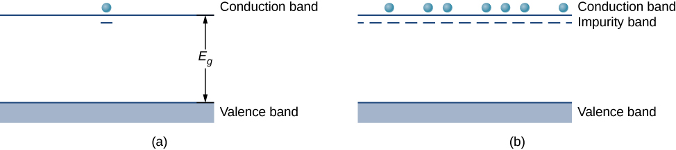
By adding more donor impurities, we can create an impurity band , a new energy band created by semiconductor doping, as shown in [link] (b). The Fermi level is now between this band and the conduction band. At room temperature, many impurity electrons are thermally excited into the conduction band and contribute to the conductivity. Conduction can then also occur in the impurity band as vacancies are created there. Note that changes in the energy of an electron correspond to a change in the motion (velocities or kinetic energy) of these charge carriers with the semiconductor, but not the bulk motion of the semiconductor itself.
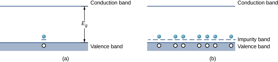
Doping can also be accomplished using impurity atoms that typically have one fewer valence electron than the semiconductor atoms. For example, Al, which has three valence electrons, can be substituted for Si, as shown in [link] (b). Such an impurity is known as an acceptor impurity , and the doped semiconductor is called a p -type semiconductor , because the primary carriers of charge (holes) are positive. If a hole is treated as a positive particle weakly bound to the impurity site, then an empty electron state is created in the band gap just above the valence band. When this state is filled by an electron thermally excited from the valence band ( [link] (a)), a mobile hole is created in the valence band. By adding more acceptor impurities, we can create an impurity band, as shown in [link] (b).
The electric current of a doped semiconductor can be due to the motion of a majority carrier , in which holes are contributed by an impurity atom, or due to a minority carrier , in which holes are contributed purely by thermal excitations of electrons across the energy gap. In an n -type semiconductor, majority carriers are free electrons contributed by impurity atoms, and minority carriers are free electrons produced by thermal excitations from the valence to the conduction band. In a p -type semiconductor, the majority carriers are free holes contributed by impurity atoms, and minority carriers are free holes left by the filling of states due to thermal excitation of electrons across the gap. In general, the number of majority carriers far exceeds the minority carriers. The concept of a majority and minority carriers will be used in the next section to explain the operation of diodes and transistors.
In studying p - and n -type doping, it is natural to ask: Do “electron holes” really act like particles? The existence of holes in a doped p -type semiconductor is demonstrated by the Hall effect. The Hall effect is the production of a potential difference due to the motion of a conductor through an external magnetic field (see The Hall Effect ). A schematic of the Hall effect is shown in [link] (a). A semiconductor strip is bathed in a uniform magnetic field (which points into the paper). As the electron holes move from left to right through the semiconductor, a Lorentz force drives these charges toward the upper end of the strip. (Recall that the motion of the positively charged carriers is determined by the right-hand rule.) Positive charge continues to collect on the upper edge of the strip until the force associated with the downward electric field between the upper and lower edges of the strip just balances the upward magnetic force . Setting these forces equal to each other, we have . The voltage that develops across the strip is therefore
Notification Switch
Would you like to follow the 'University physics volume 3' conversation and receive update notifications?

|
|

|
|

|
|
|
|
|
|
|

|
|

|
|

|
|

|
|
|
|