

| << Chapter < Page | Chapter >> Page > |
The diode is the simplest semiconductor device, made up of a p-type semiconductor and an n-type semiconductor in contact. It can conduct in only one direction, but it cannot control the size of an electric current. Transistors are more complicated electronic components which can control the size of the electric current flowing through them.
This enables them to be used in amplifiers. A small signal from a microphone or a radio antenna can be used to control the transistor. In response, the transistor will then increase and decrease a much larger current which flows through the speakers.
One of the earliest popular uses of transistors was in cheap and portable radios. Before that, radios were much more expensive and contained glass valves which were fragile and needed replacing. In some parts of the world you can still hear people talking about their `transistor' — they mean their portable radio.
You can also use a small current to turn the transistor on and off. The transistor then controls a more complicated or powerful current through other components. When a transistor is used in this way it is said to be in switching mode as it is acting as a remotely controlled switch. As we shall see in the final sections of this chapter, switching circuits can be used in a computer to process and store digital information. A computer would not work without the millions (or billions) of transistors in it.
There are two main types of transistor - bipolar transistors (NPN or PNP), and field effect transistors (FETs). Both use doped semiconductors, but in different ways. You are mainly required to know about field effect transistors (FETs), however we have to give a brief description of bipolar transistors so that you see the difference.
Bipolar transistors are made of a doped semiconductor `sandwich'. In an NPN transistor, a very thin layer of p-type semiconductor is in between two thicker layers of n-type semiconductor. This is shown in [link] . Similarly an PNP transistor consists of a very thin n-type layer in between two thicker layers of p-type semiconductor.
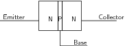
In an NPN transistor a small current of electrons flows from the emitter (E) to the base (B). Simultaneously, a much larger current of electrons flows from the emitter (E) to the collector (C). If you lower the number of electrons able to leave the transistor at the base (B), the transistor automatically reduces the number of electrons flowing from emitter (E) to collector (C). Similarly, if you increase the current of electrons flowing out of the base (B), the transistor automatically also increases the current of electrons flowing from emitter (E) to collector (C). The transistor is designed so that the current of electrons from emitter to collector ( ) is proportional to the current of electrons from emitter to base ( ). The constant of proportionality is known as the current gain . So .
How does it do it? The answer comes from our work with diodes. Electrons arriving at the emitter (n-type semiconductor) will naturally flow through into the central p-type since the base-emitter junction is forward biased. However if none of these electrons are removed from the base, the electrons flowing into the base from the emitter will fill all of the available `holes'. Accordingly, a large depletion band will be set up. This will act as an insulator preventing current flow into the collector as well. On the other hand, if the base is connected to a positive voltage, a small number of electrons will be removed by the base connection. This will prevent the `holes' in the base becoming filled up, and no depletion band will form. While some electrons from the emitter leave via the base connection, the bulk of them flow straight on to the collector. You may wonder how the electrons get from the base into the collector (it seems to be reverse biased). The answer is complicated, but the important fact is that the p-type layer is extremely thin. As long as there is no depletion layer, the bulk of the electrons will have no difficulty passing straight from the n-type emitter into the n-type collector. A more satisfactory answer can be given to a university student once band theory has been explained.
Notification Switch
Would you like to follow the 'Siyavula textbooks: grade 12 physical science' conversation and receive update notifications?

|
|

|
|
|
|
|

|
|

|
|

|
|
|
|
|

|
|

|
|

|