<< Chapter < Page Chapter >> Page >

Intrinsic properties and doping

We have seen that the size of the energy gap between the valence band and the conduction band determines whether a solid is a conductor or an insulator. However, we have seen that there is a material known as a semi-conductor. A semi-conductor is a solid whose band gap is smaller than that of an insulator and whose electrical properties can be modified by a process known as doping .

Doping

Doping is the deliberate addition of impurities to a pure semiconductor material to change its electrical properties.

Semiconductors are often the Group IV elements in the periodic table. The most common semiconductor elements are silicon (Si) and germanium (Ge). The most important property of Group IV elements is that they have 4 valence electrons.

Band gaps of si and ge

Si has a band gap of 1 . 744 × 10 - 19  J while Ge has a band gap of 1 . 152 × 10 - 19  J.

So, if we look at the arrangement of for example Si atoms in a crystal, they would look like that shown in [link] .

Arrangement of atoms in a Si crystal.

The main aim of doping is to make sure there are either too many (surplus) or too few electrons (deficiency). Depending on what situation you want to create you use different elements for the doping.

Surplus

A surplus of electrons is created by adding an element that has more valence electrons than Si to the Si crystal. This is known as n-type doping and elements used for n-type doping usually come from Group V in the periodic table. Elements from Group V have 5 valence electrons, one more than the Group IV elements.

A common n-type dopant (substance used for doping) is arsenic (As). The combination of a semiconductor and an n-type dopant is known as an n-type semiconductor. A Si crystal doped with As is shown in [link] . When As is added to a Si crystal, 4 of the 5 valence electrons in As bond with the 4 Si valence electrons. The fifth As valence electron is free to move around.

It takes only a few As atoms to create enough free electrons to allow an electric current to flow through the silicon. Since n-type dopants `donate' their free atoms to the semiconductor, they are known as donor atoms .

Si crystal doped with As. For each As atom present in the Si crystal, there is one extra electron. This combination of Si and As is known as an n-type semiconductor, because of its overall surplus of electrons.

Deficiency

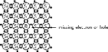
A deficiency of electrons is created by adding an element that has less valence electrons than Si to the Si crystal. This is known as p-type doping and elements used for p-type doping usually come from Group III in the periodic table. Elements from Group III have 3 valence electrons, one less than the semiconductor elements that come from Group IV. A common p-type dopant is boron (B). The combination of a semiconductor and a p-type dopant is known as an p-type semiconductor. A Si crystal doped with B is shown in [link] . When B is mixed into the silicon crystal, there is a Si valence electron that is left unbonded.

The lack of an electron is known as a hole and has the effect of a positive charge. Holes can conduct current. A hole happily accepts an electron from a neighbor, moving the hole over a space. Since p-type dopants `accept' electrons, they are known as acceptor atoms .

Si crystal doped with B. For each B atom present in the Si crystal, there is one less electron. This combination of Si and B is known as a p-type semiconductor, because of its overall deficiency of electrons.

Donor (n-type) impurities have extra valence electrons with energies very close to the conduction band which can be easily thermally excited to the conduction band. Acceptor (p-type) impurities capture electrons from the valence band, allowing the easy formation of holes.

The energy level of the donor atom is close to the conduction band and it is relatively easy for electrons to enter the conduction band. The energy level of the acceptor atom is close to the valence band and it is relatively easy for electrons to leave the valence band and enter the vacancies.

Intrinsic properties and doping

  1. Explain the process of doping using detailed diagrams for p-type and n-type semiconductors.
  2. Draw a diagram showing a Ge crystal doped with As. What type of semiconductor is this?
  3. Draw a diagram showing a Ge crystal doped with B. What type of semiconductor is this?
  4. Explain how doping improves the conductivity of semi-conductors.
  5. Would the following elements make good p-type dopants or good n-type dopants?
    1. B
    2. P
    3. Ga
    4. As
    5. In
    6. Bi

Questions & Answers

what is phylogeny
Odigie Reply
evolutionary history and relationship of an organism or group of organisms
AI-Robot
ok
Deng
what is biology
Hajah Reply
the study of living organisms and their interactions with one another and their environments
AI-Robot
what is biology
Victoria Reply
HOW CAN MAN ORGAN FUNCTION
Alfred Reply
the diagram of the digestive system
Assiatu Reply
allimentary cannel
Ogenrwot
How does twins formed
William Reply
They formed in two ways first when one sperm and one egg are splited by mitosis or two sperm and two eggs join together
Oluwatobi
what is genetics
Josephine Reply
Genetics is the study of heredity
Misack
how does twins formed?
Misack
What is manual
Hassan Reply
discuss biological phenomenon and provide pieces of evidence to show that it was responsible for the formation of eukaryotic organelles
Joseph Reply
what is biology
Yousuf Reply
the study of living organisms and their interactions with one another and their environment.
Wine
discuss the biological phenomenon and provide pieces of evidence to show that it was responsible for the formation of eukaryotic organelles in an essay form
Joseph Reply
what is the blood cells
Shaker Reply
list any five characteristics of the blood cells
Shaker
lack electricity and its more savely than electronic microscope because its naturally by using of light
Abdullahi Reply
advantage of electronic microscope is easily and clearly while disadvantage is dangerous because its electronic. advantage of light microscope is savely and naturally by sun while disadvantage is not easily,means its not sharp and not clear
Abdullahi
cell theory state that every organisms composed of one or more cell,cell is the basic unit of life
Abdullahi
is like gone fail us
DENG
cells is the basic structure and functions of all living things
Ramadan
What is classification
ISCONT Reply
is organisms that are similar into groups called tara
Yamosa
in what situation (s) would be the use of a scanning electron microscope be ideal and why?
Kenna Reply
A scanning electron microscope (SEM) is ideal for situations requiring high-resolution imaging of surfaces. It is commonly used in materials science, biology, and geology to examine the topography and composition of samples at a nanoscale level. SEM is particularly useful for studying fine details,
Hilary
Got questions? Join the online conversation and get instant answers!
Jobilize.com Reply

Get Jobilize Job Search Mobile App in your pocket Now!

Get it on Google Play Download on the App Store Now


Source:  OpenStax, Siyavula textbooks: grade 11 physical science. OpenStax CNX. Jul 29, 2011 Download for free at http://cnx.org/content/col11241/1.2
Google Play and the Google Play logo are trademarks of Google Inc.

Notification Switch

Would you like to follow the 'Siyavula textbooks: grade 11 physical science' conversation and receive update notifications?

Ask