

| << Chapter < Page | Chapter >> Page > |
Chapter 5_Section 5.1_Semi-conductor Materials and its Absorption Coefficient curves.
In Photonics we study optical energy sources and optical energy detectors/sensors. Both are diodes but they are especially constructed so that a source may emit a copious amount of optical energy and detector may absorb a 99% of the incident optical energy to produce a optimum response. The optical energy detectors are always kept reverse biased but when there is no bias then under illumination condition they can be used as photo-voltaic cells or solar cells also. The optical detectors under reverse bias detects a particular wavelength or shorter of Electro-Magnetic Radiation only when the Energy Packet of the given EM Radiation contains (hν) energy greater than the band-gap of the semiconducting material constituting the optical detectors.
There is a very convenient relationship which directly gives the threshold wavelength . Incident light shorter than this threshold wavelength will optically excite optical sensor and generate an electrical signal in response to photo-excitation. The relationship is as follows:

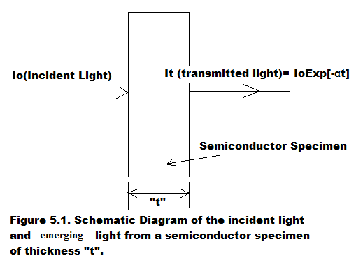
The sensitivity of the Optical Detector depends on the absorption coefficient of the material constituting the optical detector. The absorption coefficient (α per cm) is described in Figure 5.1. as formulated below:


The absorption coefficient curves are shown in Figure 5.2. for elemental semi-conductors such as Ge, Si and Hydrogenated Amorphous Si (α-Si) and for compound semiconductors such as GaAS, InP and InGaAs.
As is evident from Figure 5.2, compound semiconductors have a very sharp cut-off in absorption coefficient at wavelengths larger than threshold wavelength.
GaAs has a Band-Gap of 1.42eV which gives a threshold wavelength of 0.87μm from Equation 5.1. Hence for wavelengths longer than 0.87μm, GaAs is transparent. Light passes through a specimen of GaAs unobstructed at wavelengths longer than 0.87μm. At 0.87μm the specimen becomes opaque and absorbs light at 0.87μm and shorter wavelengths.
The reciprocal of the absorption coefficients is penetration depth as defined below:

Penetration Depth tells that the thickness of GaAs detector/sensor must be greater than d*= 1μm in order to fully absorb the incident photons and give a large electrical response. All compound semiconductors behave in identical manner. As is evident from Figure 5.2, GaAs, InP and InGaAs give a step jump in the absorption coefficient at and shorter wavelength than threshold wavelengths namely at 0.82μm, 0.92μm and 1.39μm respectively. For optimum electrical response the thickness of absorbing layer must be about 1μm in all three cases. Compound Semiconductor exhibit such a sharp response due to the fact that they are Direct-Bandgap Semi-conductor.
In contrast elemental semi-conductors such as Si and Ge have much softer response. In case of Si, at wavelength 1.39μm and at shorter wavelengths the response only gradually increases as a result maximum response can be obtained only if the thickness of active absorbing layer is 50μm. In case of Ge, response gradually increases at 1.88μm and at shorter wavelengths and here also the effective thickness should be of the order of 50μm. This increases the cost of the detector or photo-voltaic cell.
In Si, absorption coefficient can be vastly improved if we use hydrogenated amorphous Si(α-Si). This has an identical responsivity curve as that of GaAs hence it is the commonly used material in Solar Cells.
Notification Switch
Would you like to follow the 'Solid state physics and devices-the harbinger of third wave of civilization' conversation and receive update notifications?

|
|

|
|

|
|
|
|

|
|
|
|
|

|
|

|
|

|
|

|