

| << Chapter < Page | Chapter >> Page > |
4. Bipolar Junction Transistor.
The first 3 terminal Solid State Device to be invented and commercialized was Bipolar Junction Transistor. It was invented in 1948 and discrete Ge-BJT wre immediately mass produced. Subsequently the merits of Si-BJT were recognized and Si-BJT went into mass production for various Signal Processing Applications.In 1961 first Bipolar Si-IC also went into mass production. This was Resistance-Transistor-Logic IC. MOSFET IC's were commercialized in 1970 mainly for application in watches but subsequently they became the main stay of Micro-processors chips. NMOS was soon replaced by CMOS because of its nano-watt standby dissipation characteristics. Today the heat management problems at nano-scale has led to the adoption of CMOS ICs but BJT still finds application in very high frequency,low noise and high output power applications.It is used in mobile phone output stages. BJT Analog ICs will continue to be the interface circuits in most general applications.
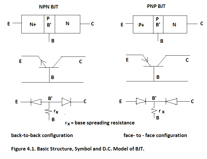
Bipolar Junction Transistor (BJT) is a back-to-back(NPN) or face-to-face device(PNP) and it is three terminal device as shown in Figure 4.1.
It has four modes of operation as given below:
Forward Active Mode: EB Jn Forward biased, BC Jn Reverse biased.
Inverse Active Mode: EB Jn Reverse biased, BC Jn Forward biased.
Saturation Mode: EB Jn Forward biased, BC Jn Forward biased.
Cut off Mode: EB Jn Reverse biased, BC Jn Reverse biased.
It can be biased as a linear device to amplify signals. It can be biased as a switch to act as Digital Logic Gate.
In Forward Mode: BJT acts like a linear device.
In Saturation Mode(short circuit) and in Cut-off Mode(open circuit) it acts like a Switch.
Figure 4.2. gives Carrier Concentration Profile in Forward Active Mode.
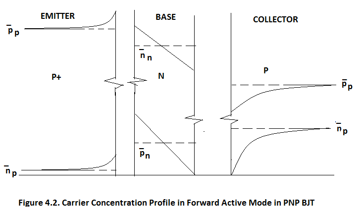
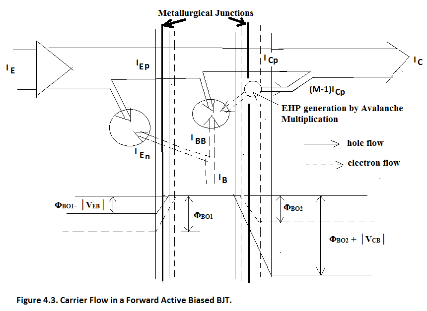
Figure 4.3. shows the carrier flow. In Figure 4.3. we note that barrier potential at Forward Biased EB Junction reduces from Φ BO1 to Φ BO1 - │V EB │ and at Reverse Biased BC junction it increases from Φ BO2 to Φ BO2 - │V CB │. Therefore holes are easily injected into the Base. The Base is very narrow, less than 1μm, hence the injected holes easily diffuse across the BASE and fall down the reverse biased BC potential gradient. Hole is minority carrier in N-Type Base hence BC Junction acts as down-hill gradient for the holes. In effect Emitter is injecting the holes into the Base and Collector is collecting the holes and holes are transiting the BASE in a finite time called Base Transit Time = τ. This Transit Time decides the Transit Frequency or the Unity Gain Frequency of the given BJT. This Transit angular Frequency ω T = (1/τ) = 2πf T . This Transit Frequency ranges from 200MHz to 800MHz for UHF BJT and it can go as high as 500GHz for Microwave Transistors.

Here γ = Injection Efficiency = I Ep /I E ;
And β*= Base Transport Factor = I Cp /I Ep ;
M= Avalanche Multiplication Factor.
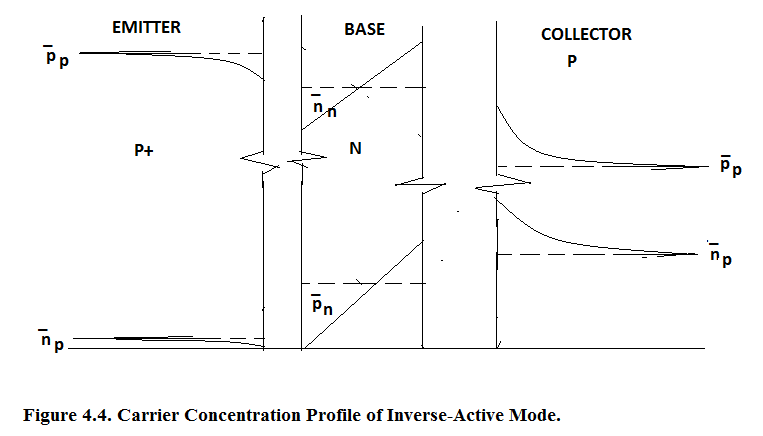
In Figure 4.4. Carrier Concentration Profile of Inverse Active Mode is shown. It is exactly the inverse of Forward Active Mode. The performance of Inverse Active Mode BJT is much inferior to that of Forward Active Mode as we will see this in the Output Family of Curve of Inverse Active Mode Common Base BJT.
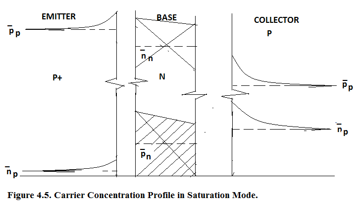
In Figure 4.5. Carrier Concentration Profile in Saturation Mode is shown. Since both junctions are forward biased hence holes are being injected from Emitter and Collector both. This leads to heavy build up and storage of minority carries. It causes a very large Storage Time Delay during switching. Hence we use Schottky Clamped BJT where deep saturation is prevented. This leads to drastic improvement in switching speed. In 70’s gold dope was used to kill the minority carruier and thereby reduce the storage delay. But it led to large reverse leakage current. Hence Schottky Clamped method was adopted for improving the switching speed.
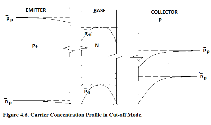
In Figure 4.6.Carrier Concentration Profile in Cut-off Mode is shown. Both Junctions are reverse biased hence no current flows..
Notification Switch
Would you like to follow the 'Solid state physics and devices-the harbinger of third wave of civilization' conversation and receive update notifications?

|
|

|
|

|
|

|
|
|
|
|
|
|
|

|
|
|
|
|
|
|
|

|