

| << Chapter < Page | Chapter >> Page > |
Although lapping would appear to be simple in concept, the successful implementation of a production lapping operation requires the development of a technique and experience to achieve acceptable quality with good yields. Small adjustments to the rotation rates of the plates and carriers will cause the plates to wear concave, convex or flat.
As lapping is a messy process, various efforts have been made to avoid it or to substitute an alternative process. The most likely approach at present is grinding, in which the wafer is held on a vacuum chuck and a series of progressively finer diamond wheels is moved over the wafer while it is rotated on a turn table. Grinding gives a clearer surface than lapping, however, only one side may be ground at a time and the resulting flatness is not as good as that obtained by lapping.
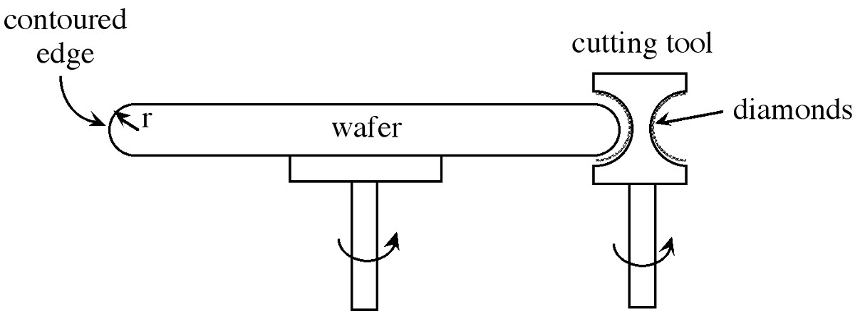
The rounding of the edge of the wafer to a specific contour is a fairly recent development in the technology of wafer preparation. It was known by the early seventies that a significant number of device yield problems could be traced to the physical condition of the wafer edge. An acute edge affects the strength of the wafer due to: stress concentration, and a lowering of its resistance to thermal stress, as well as being the source of particle chip, breakage, and lattice damage. In addition, the particles originating from the chipped edges can, if present on the wafer surface, add to the defect density (D 0 ) of the IC process reducing fabrication yield. Further problems associated with a square edge include the build-up of photoresist at the wafer edge. The solution to these process problems is to provide a contoured edge with a defined radius (r).
Chemical etching of wafers results in a degree of edge rounding, but it is difficult to control. Thus, mechanical edge contouring has been developed and the result has been a dramatic improvement in yields in downstream wafer processing. Losses due to wafer breakage are also reduced. The edge contouring process is usually performed in cassette-fed high speed equipment, in which each wafer is rotated rapidly against a shaped cutting tool ( [link] ).
The mechanical processes described above to shape the wafer leave the surface and edges damaged and contaminated. The depth of the work damage depends on the specific process, however, 10 μm is typical. Such damage is readily removed by chemical etching. Etching is used at multiple points during the fabrication of a semiconductor device. The discussion below is limited to etches suitable for wafer fabrication, i.e., non-selective etching of the entire wafer surface.
The wet chemical etching of any material can be considered to involve three steps: (a) transportation of the reactants to the surface, (b) reaction at the surface, and (c) movement of the reaction products into the etchant solution ( [link] ). Each of these may be the rate limiting step and thus control the etch rate and uniformity. This effect is summarized in [link] .
Notification Switch
Would you like to follow the 'Chemistry of electronic materials' conversation and receive update notifications?

|
|

|
|
|
|

|
|

|
|

|
|

|
|

|
|

|
|

|