

| << Chapter < Page | Chapter >> Page > |
SSPD_Chapter 7_Part 3_Basic Electrical Properties of MOSFETcontinued 6
7.3.13. MOS Transistor’s parasitic capacitances.
Just as parasitic capacitances C µ and C π limit the frequency reponse of BJT in exactly the identical manner gate oxide capacitances limit the frequency response of MOSFET.
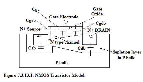
Referring to Figure 7.3.13.1. we identify the following capacitances:
C GC = gate to channel capacitance,
C GSO = gate to source overlap capacitance and
C GDO = gate to drain overlap capacitance.
Overlap capacitances occur mainly due to:
Because of self aligned processing, C GSO and C GDO are minimized. C GC has the dominant contribution in limiting the frequency response.
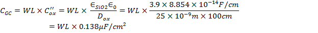
Typical value of channel-gate capacitance is:
7.3.13.1. Capacitance in Triode Region.
We effectively have C GS and C GD in Triode region of MOSFET. The contribution of C GC is included in these two capacitances.
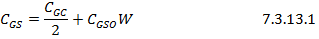
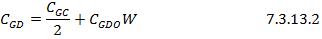
Note that C OX ” is Farad per unit area whereas overlap capacitance is Farad per unit length.
As seen in the Figure 7.3.13.1, in addition to the above capacitances , there is Source to Bulk capacitance (C SB ) and Drain to Bulk capacitance (C DB ) due to the depletion layer surrounding the Source and Drain. The reverse biased junction exists at the bottom of the source and drain. It also exists at the periphery of the source and the drain.
Source-to-Bulk capacitance =


P S and P D are the perimeters of Source and Drain.
A S and A D are the bottom area of Source and Drain.
C j and C jSW are dependent on the reverse voltage existing between the Source(or Drain) and the bulk because junction capacitance is proportional to CS area/ depletion width and depletion width varies the square root of the reverse voltage in step kunction and it depends on the cube root of the reverse voltage in linearly graded junction.
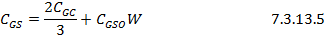
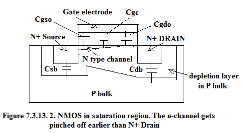
7.3.13.2. Capacitances in Pentode or Saturation Region.
In saturation region, there is no channel on the drain side hence Gate-Channel capacitance has no contribution to Gate-Drain Capacitance. Therefore:

7.3.13.2. Capacitances in Cut-off Region.
Figure 7.3.13.3 gives the cross-sectional area of NMOS which is below the threshold region hence it is in cut-off region. In cut-off region there is no channel hence no gate-channel capacitance.


C GBO = Gate-Bulk Capacitance per unit width.
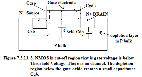
Generally in Digital Systems we will encounter Saturation and Cut-off conditions hence capacitance s showed in Figure 7.3.13.2 and in Figure 7.3.13.3 will be relevant to us in course of analysis.
Notification Switch
Would you like to follow the 'Solid state physics and devices-the harbinger of third wave of civilization' conversation and receive update notifications?

|
|

|
|

|
|

|
|

|
|
|
|
|

|
|

|
|

|
|

|