

| << Chapter < Page | Chapter >> Page > |
SSPD_Chapter 7_Part 3_Basic Electrical Properties of MOS and MOS circuits.
7.3 The Output Characteristics of (Depletion)n-channel MOSFET.
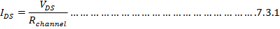
Field Effect Transistors cover JFET and MOSFET. The underlying principle of FET is that there is a conducting channel which obeys Ohm’s Law:
Where
L = lemgth of the channel and A = cross-sectional area as shown in Figure 7.3.1.
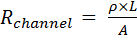
And ρ = resistivity = 1/σ = 1/conductivity = 1/(qµ n n);
Here q = charge of an electron, µ n = mobility of an electron in the channel and n = conducting electron density in the n-channel.
Generally the n-channel is like a 2-D sheet hence its mobility is much lower than that in 3-D bulk. Typically µ n = 1450 cm 2 /(V-sec) in Bulk Semiconductor and 650 cm 2 /(V-sec) in the channel in FET.
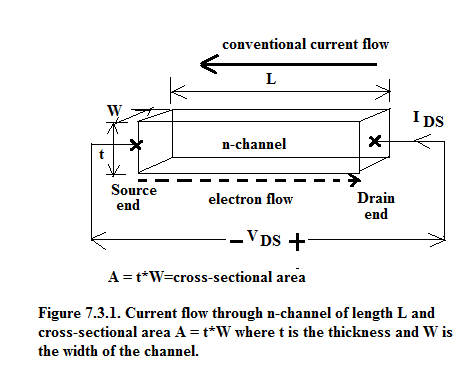
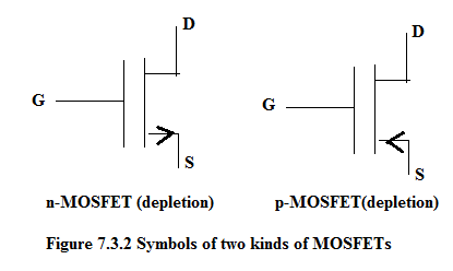
As can be seen in the Figure 7.3.1 in n-channel FET electrons are being sourced from the source end and being drained out from the drain end. By corollary in p-channel FET holes will be sourced and holes will be drained out. This is the reason why the symbols are shown with the arrow of the conventional current flow. In nMOSFET conventional current is shown to come out of the Source and in pMOSFET conventional current is shown to enter into the Source as shown in Figure 7.3.2.
Equation 7.3.1 is a linear equation with I-V characterisyics as shown in Figure 7.3.3.
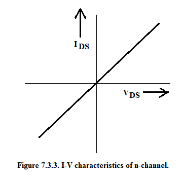
As seen in the Figure 7.3.3, I-V is linear for the whole range of voltage applied and is anti-symmetrical about the y-axis. Hence n-channel is a bilateral device where for positive voltage positive current flows and for negative voltage negative current flows with equal ease.
7.3.1. FET as a 3-terminal Device in Ohmic Region/Triode Region
Now by applying GATE voltage V GS transverse to the channel as shown in Figure 7.3.4 the channel thickness can be controlled and thereby the I-V slope can be controlled as shown in Figure 7.3.5.
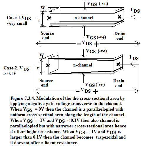
In this OHMIC REGION of operation, we have two cases. First case is when V DS is kept less than 0.1V. In this case channel remains a parrallaelopied with a reduced thickness ‘t’. In this case if we continue to apply more and more negative voltage, the channel will be eventually be completed depleted and we say that the channel has pinched off. The negative gate voltage at which this occurs is known as Pinch-Off voltage (V P ).
There is a second case where V DS is greater than 0.1V and it continues to be increased. In this case the difference voltage between Gate and Drain>the difference between Gate and Source. Hence n-channel is trapezoidal and it does not give a linear I-V characteristics. This is also OHMIC REGION but non-linear. Linear and non-linear I-V curve is clearly indicated in Figure 7.3.5.
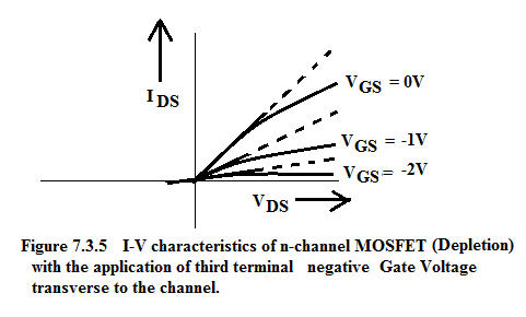
As seen in Figure 7.3.4 and Figure 7.3.5 we have achieved Voltage –Controlled Resistance (VCR) but this VCR is not quite linear. At V DS <0.1V, VCR is perfectly linear but at large V DS voltages the channel resistance deviates from the linear behavior.
In this kind of device at zero gate voltage, channel is present. Hence it is known as Normally-On . As the negative gate voltage is made more negative, the channel depletes until it finally completely pinches off . Hence it is known as .Depletion Type Device. As the gate voltage is made positive, channel becomes more conductive as it has a copious supply of electrons. Theefore we say that n-channel has enhanced.
Notification Switch
Would you like to follow the 'Solid state physics and devices-the harbinger of third wave of civilization' conversation and receive update notifications?

|
|

|
|

|
|

|
|

|
|

|
|

|
|
|
|

|
|

|