

| << Chapter < Page | Chapter >> Page > |
SSPD_Chapter 7_Part 7_Scaling of MOS circuits_concluded.
7.7.8. Definition of half pitch and node.
International Technology Roadmap for Semiconductors uses ‘node’ to refer to the smallest feature size on Logic Chips. This is the length of the Gate of MOSFET. Whereas in Memory Chips ‘half pitch’ is used to define the smallest feature size.
Half-pitch is the half distance between two adjacent aluminium pathways. Nodes and half-pitch are illustrated in Figure 7.7.8.1
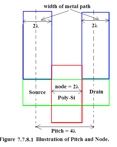
As is evident from the figure, Half-Pitch = Node. But with the evolution of Technology the MOS structure has been modified and today Half-Pitch>Node. In Figure 7.7.8.2 we see the evolution of MOS structure from 1970 to 2005.
As we see that with scaling LDD(Lightly Doped Drain) had to be introduced under the edges of the Gate to mitigate the short channel effect. With the scaling of the dimensions, V DD was not proportionately scaled down under General Scaling Scheme as a result sharp electric field is created which results in “hot electrons effect”. Hot Electron Effects has deleterious effects on the Device. These are the following:
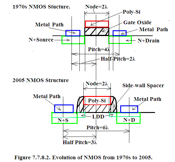
To mitigate the short channel effects we introduce Side-Wall Spacer at the edges of the Poly-Si Gate and LDD(Lightly Doped Drain) on source and drain side as shown in the lower half of Figure 7.7.8.2.. LDD extends below the the edge of the Poly-Si Gate. This has been achieved by tilted angle implant.
By grading the doping of Drain and Source from N+ to N- (LDD), we allow a more gradual drop of voltage leading to the reduction in the peak of the electric field along the channel. Even modest reduction in field leads to significant improvement in the performance of the device. It suppresses the hot electron generation, it prevents the saturation of the drift velocity of the electrons in the channel and the shallow junction of LDD helps minimize the chanel length modulation parameter.
The net result of this modification has been that in recent years Half-Pitch>Node as seen in the following tables.
Notification Switch
Would you like to follow the 'Solid state physics and devices-the harbinger of third wave of civilization' conversation and receive update notifications?

|
|

|
|

|
|

|
|

|
|

|
|

|
|

|
|

|
|

|