

| << Chapter < Page | Chapter >> Page > |
SSPD_Chapter 7_Part 6_Basic Circuit Concepts_continued 5
7.6.6. Super buffers for driving significant capacitive loads.
To drive significant capacitive loads we use super buffers to preserve symmetric switching transients. This considerably minimizes the delay problems. The circuit diagrams of inverting type super buffers is given in Figure 7.6.6.1 and that of non-inverting type in Figure 7.6.6.2.
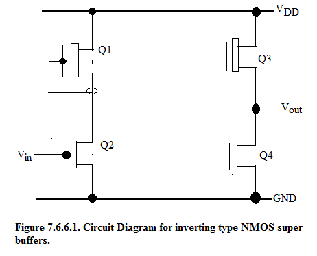
In Figure 7.6.6.1. Q1-Q2 comprise (E)NMOS inverter with (D)NMOS acting as pull-up transistor. The output of the inverter drives the gate of Q3 and original input drives the gate of Q4.
When V in = HIGH (V DD ), inverter O/P is LOW which pulls down the gate of Q3 to 0V thereby Q3 is turned OFF but Q4 is turned ON. Hence O/P of the super buffer is rapidly pulled down through Q4.
When V in = LOW (0V), inverter O/P is HIGH. Original input turns OFF the pd transistor Q4 but HIGH O/P of the inverter turns ON the pu transistor Q3. Thus O/P of the super buffer is rapidly pulled up through Q3.
Note that in the conventional inverter under pu condition V DD /2 is applied at the gate of pu transistor. In case of super buffer, V DD is being applied to the gate of pu transistor Q3. Hence in the second case pu transistor is being turned ON twice as hard as in the conventional case. Hence pu is twice as rapid. This helps symmetrize the output transients.
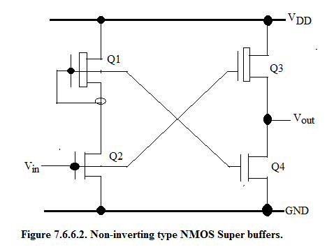
In Figure 7.6.6.2. we have non-inverting type super buffers. It is the same as inverting type except that the inveter output is cross-coupled to Q3-Q4 pair.
Hence when Vin = HIGH, O/P of the buffer is being pulled up through Q3.
When Vin = LOW, O/P is being pulled down through Q4.
Thus Vin = HIGH gives buffer O/P =HIGH and
Vin=LOW gives buffer O/P= LOW.
7.6.7.BICMOS Drivers.
BJT Logic has much better drive capabilities as compared to CMOS Logic.
Because of these reasons BJT drive at the output of CMOS is preferred hence it is called GLUE Logic.
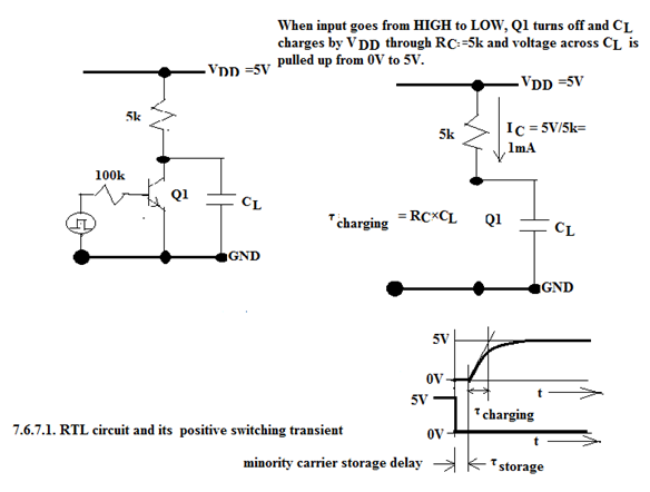
In Figure 7.6.7.1, Resistance-Transistor –Logic (RTL) circuit configuration is shown. Along side the positive switching transient at the output is shown with input experiencing 5V negative step. When I/P goes HIGH to LOW, transistor is first switched OFF. Because the transistor was in saturation therefore it takes time to remove all the stored minority carriers in the base. This causes storage delay ,τ(storage).
Once the transistor is turned OFF, the load capacitance is pulled up through load resistance R C . Hence the charging time constant τ(charging) = R C ×C L . The pull-up tramsient with storage delay is shown at the bottom right of the diagram.
In Figure 7.6.7.2 we show the negative transient across the capacitive load at the output of the RTL gate.
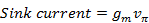
The input is HIGH at 5V hence transitor is ON and sink current is caused :
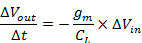
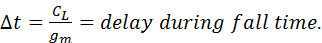
Therefore the rate of pull-down across the capacitor is:

This can be rewritten as:
In Logic Gates :
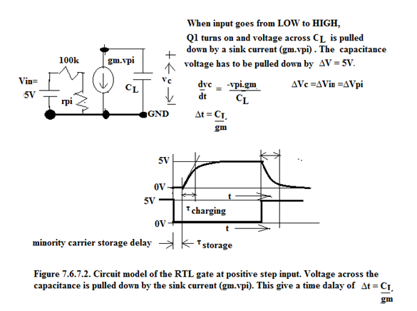
Therefore
This clearly shows the delay dependence on transconductance. BJT has a much larger transconductance and therefore delay will be minimized using BICMOS.
So finally the total delay factors in BICMOS are:
Minority carrier storage delay (t1)+
Charging delay or pull up delay+
Discharging delay or pull down delay.
In Figure 7.6.7.3 we make a comparative study of the delays in BiCMOS and CMOS inverters.
Total delay of BiCMOS is given by the following expression:
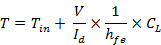
Where T = total delay; T in = time to charge BE Junction capacitance; hfe= short circuit current gain.
In Figure 7.6.7.3 we give two graphs. Upper Graph is the delay performance of BiCMOS and CMOS gates with respect to load capacitance. Lower Graph is the delay performance of BiCMOS with respect to collector resistance R C for two different values of C L .
From the upper graph it is evident that after a critical value of C L , BiCMOS switching is much faster than CMOS and it gives increasingly better performance as C L increases .
The lower graph shows the necessity of keeping collector resistance low so that the pull-up of capacitive load is rapid. This also is the reason why buried sub-collector layer is included in the BJT structure.
Because BiCMOS can achieve high grade BJT with high gm, high short circuit current gain and low bulk collector resistance hence BJT is included in CMOS fabrication without compromising or overelaborating the basic CMOS process.
Notification Switch
Would you like to follow the 'Solid state physics and devices-the harbinger of third wave of civilization' conversation and receive update notifications?

|
|

|
|
|
|

|
|

|
|

|
|

|
|

|
|

|
|

|