

| << Chapter < Page | Chapter >> Page > |
SSPD_Chapter 7_Part 2_BiCMOS Technology
7.2 In SSPD_Chapter 6_Part 6 we have extensively discussed CMOS Process Flow and CMOS fabrication technology. Here we deal with BiCMOS Technology. In Figure 7.2.1 we give the speed-power performance of available technologies.
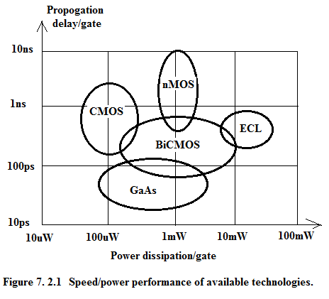
Here we will do a rapid review of the Logic Families available in the market. Figure 7.2.2 gives the broad classification of the Logic Families. From the graph in Figure 7.2.1 it is evident that GaAs is the fastest Logic Family and CMOS is the slowest but consumes nW power and has a very high packing density hence CMOS is the technology of choice for microprocessor and microcontroller.
CMOS has one serious drawback and that is its limited driving capability. To overcome this problem one could use CMOS with super-buffers using MOS transistors alone. But still it does not compare well with BiCMOS in output drive circuits.. As seen in Figure 7.2.1, BiCMOS is faster than CMOS though dissipating more power.
CMOS and Bipolar Technology have their own advantages as shown in Table 7.2.1. BiCMOS combines the virtues of both the technology.
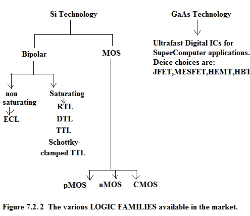
Table 7.2.1. Comparison between CMOS and Bipolar Technologies.
| CMOS Technology | BJT Technology |
| Nano-watt logic. It has nano-watt standby power dissipation | Milli-watt standby power |
| High Zin hence low drive current | Low Zin hence high drive current |
| Scalable Threshold Voltage | Low Voltage swing |
| Noise Margin is large | Noise Margin is small |
| High packing density | Low packing density because of isolation diffusion |
| Low output drive current | High output drive current. |
| Low transconductance, gm | High gm |
| Low transit frequency | High transit frequency at low currents |
| Bidirectional capability-source and drain are interchangeable | Unidirectional from input to output |
| Near Ideal Switch |
7.2.1. Process Technology of BiCMOS.
The plan view and the cross-sectional view of a BiCMOS npn transistor is shown in Figure 7.2.3.
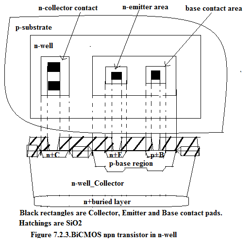
CMOS process flow can easily be extended to include bipolar NPN transistor. In the twin-tub process we will use N-tub for realizing NPN BJT. To reduce the collector series resistance, n+ buried layer is provided just below the n-tub. In addition p-base region is implanted in n-well region. Next n+ implantation is done for collector contact and for emitter region. Finally p+ is implanted as shown to make contact to the base region. Next contact pads are added to the collector contact area, emitter area and base contact area as black rectangles.
Including NPN BJT causes a loss of packing density and higher cost per gate.
By using this mix of technology we can realize complex systems in an optimal manner. In the mix, we have the option of CMOS, BiCMOS and ECL.
CMOS will be confined to logic circuitary.
BiCMOS for input/output and driver circuits.
ECL for critical high speed parts.
Notification Switch
Would you like to follow the 'Solid state physics and devices-the harbinger of third wave of civilization' conversation and receive update notifications?

|
|

|
|

|
|

|
|
|
|
|

|
|

|
|

|
|

|
|

|