

| << Chapter < Page | Chapter >> Page > |
SSPD_Chapter 7_part 5_Stick Diagrams of CMOS Gates_concluded.
7.5.4. CMOS Transmission Gate.
Figure 7.5.4.1 gives the layout of transmission switch and its stick diagram.
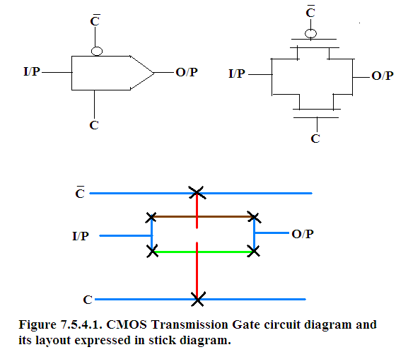
Blue- metal 1, Red – Poly-Si, Green – N+diffusion for (E)NMOS; Brown – P+diffusion.
Whenever control I/P ‘C’ = 1, ‘C complement’=0. Both the transistors turn ON and there is full transmission from I/P to O/P.
Whenever ‘C’= 0, ‘C complement’= 1 then both transistors turn ‘OFF’ and the transmission is stopped between I/P and O/P.
7.5.5. CMOS 2-input Multiplexer.
Figure 7.5.5.1 gives the Symbol and the layout of 2-input multiplexer expressed as stick disagram.
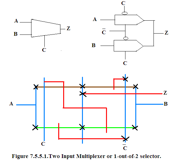
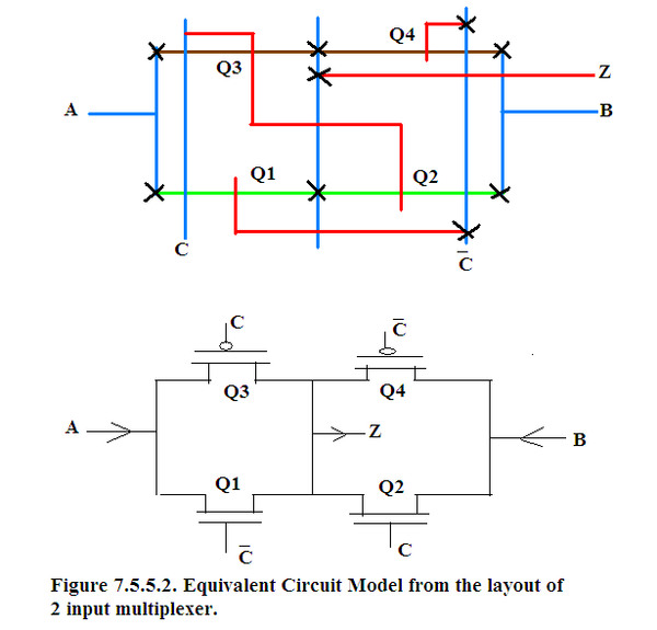
The circuit model of the layout is given in Figure 7.5.5.2.
By inspection of the circuit model we see that
when control input C=’1’ then Z = B and
when C= ‘0’ then Z = A.
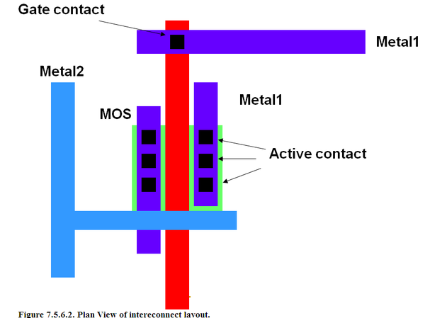
Metal layers are electrically isolated from each other. Electrical contact between
adjacent conducting layers requires contact cuts and vias.

Notification Switch
Would you like to follow the 'Solid state physics and devices-the harbinger of third wave of civilization' conversation and receive update notifications?

|
|

|
|

|
|

|
|

|
|

|
|

|
|

|
|

|
|

|