

| << Chapter < Page | Chapter >> Page > |
SSPD_Chapter 7_Part 3_Basic Electrical Properties of MOSFET_concluded.
7.3.16. Latch-Up problem in CMOS and its remedy.
[This part is adapted from the lecture series of Steve McGarry,Department of Electronics, University of Carleton, Ottawa. e-mail:smcgarry@doe.carleton.ca]
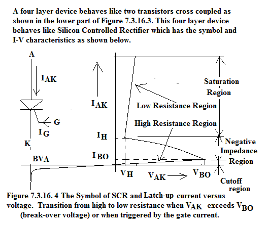
CMOS logic is fabricated either by P-Well or N-Well Process or by Twin-Well Process. In any of these processes we have a large number of junctions as . In Figure 7.3.16.1. we give the cross-sectional view of CMOS fabricated by N-Well process. These multiple junctions give rise to three-junction four-layer device which behaves like a SCR. This we call parasitic SCR.
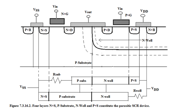
This arises due to cross coupling of P+NP and N+PN transistors. How these parasitic transistors action arise is shown in Figure 7.3.16.2.
If this parasitic SCR is turned ON by the glitches on the power bus or by irradiation, then a low resistance conducting path is created between Positive Voltage Bus (V DD ) and GND Bus (V SS ). This causes irreversible damage to the IC chip. This precisely is SCR Latch-Up problem in CMOS. By careful control during fabrication, the parasitic SCR can be prevented from latching up under all conditions.
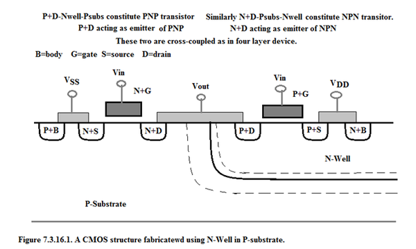
In MOS structures the source is always shorted to the body. As seen in the above Figures, Source of NMOS i.e. N+S is connected to P+body by a metal interconnect and P+body makes an ohmic contact to P-substrate. Similarly Source of PMOS i.e. P+S is connected to N+body by a metal interconnect and N+body makes an ohmic contact to N-Well. This ensures that Source-Body bias is zero which leads to zero BODY EFFECT hence threshold voltage of the MOS is held constant.
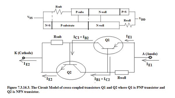
The equivalent circuit model is given in Figure 7.3.16.3.
As seen in the Figure, the positive voltage bus acts as the Anode of the parasitic SCR and the GND bus i.e. V SS bus acts as the Cathode of the parasitic SCR. For discussion purpose we assume that R substrate and R well are infinite . Under normal condtions voltage between the two buses is 5V or less hence SCR doesnot fire and there is no latching.
7.3.16.1. Why does SCR fire above break-over voltage ?
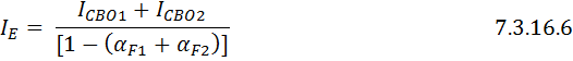
By inspection of the Circuit Model of SCR in Figure 7.3.16.3 we get the following equations:


We further see that:


Where I CBO = Collector-Base Junction reverse leakage current with Emitter open.
Adding the two above equations, we get:

By rearranging the terms we get:

We know that I E1 = I E2 = I E by Kirchoff’s Current Law;
Also I C1 + I C2 = I E2 = I E ;
Therefore rearranging the terms we get:
Forward Current Transfer Ratio of BJT is α F = γ×β*×M
Where γ = injection efficiency. It falls at low currents due to recombination in depletion layer and it also falls at high current due to conductivity modulation. It is at the maximum value at moderate currents.
Also β* = base transport factor. This improves as Base Width becomes narrower which it will at higher voltages of V CE (forward active mode).
Notification Switch
Would you like to follow the 'Solid state physics and devices-the harbinger of third wave of civilization' conversation and receive update notifications?

|
|

|
|
|
|
|

|
|

|
|

|
|

|
|

|
|

|
|

|