

| << Chapter < Page | Chapter >> Page > |
SSPD_Chapter 6_Part 6_MOS ICs Fabrication Technology_to be continued2
Section 6.6.2.4 Process Options for Active Region and Well Formation.
There are many options for Well Formation but here we will consider only two options which are commonly used by the Industries. First option is “Field Implants under LOCOS region”. This option is a more reliable method of lateral isolation of the active MOS. Second option is “Buried and Epitaxial Layer”. The second option prevents Latching of MOS through parasitic BJT formation.
Option 1. “Field implants under LOCOS region”.
In the CMOS process flow till now, the implant energies of P and N tubs were carefully chosen to penetrate the thick field oxide. Implants would be masked only in fixed KPR covered area. When the implant penetrates the field oxide, it increases the substrate doping underneath the LOCOS region and prevents the formation of inversion layer under normal voltage condition. Thus field oxide isolation is achieved. But the stopping by thick oxide is statistical in nature. Hence the dose which needs to be implanted underneath the field oxide is not achieved while the well implant is taking place. To ensure an implant under the field oxide this implant has to be carried out in a separate step.
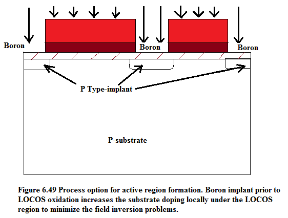
In Section 6.4.3 , Figure 6.7, the middle diagram contains the windows for local oxidation. The active regions are shielded by KPR/Si 3 N 4 /SiO 2 .Now Boron ions of implant dose of 1×10 13 cm -2 at 50keV is used for field implant. The implant energy will make the Boron ions pass through thin SiO 2 region but will be completely stopped by KPR/Si 3 N 4 /SiO 2 stack. The LOCOS region acquires a shallow P-type implant as shown in Figure 6.49.
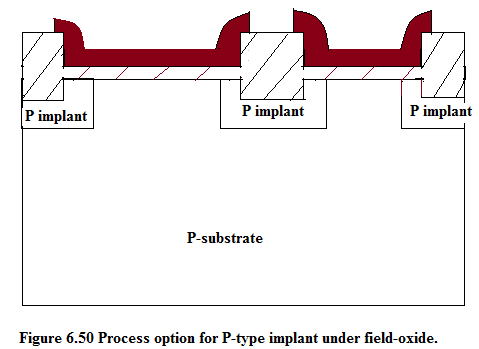
After the P-type implant we remove the fixed KPR by oxygen plasma or by an organic solvent known as stripper. Next we do the Local Oxidation through the aperture in Si 3 N 4 . The structure obtained is shown in Figure 6.50.
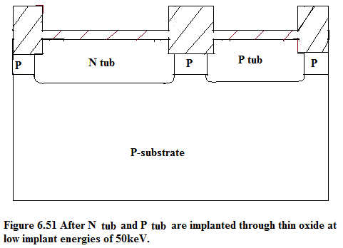
By dry etching Si3N4 is removed. Now we follow the steps in Figure 6.46 and Figure 6.47. The final structure is shown in Figure 6.51.
Option 2. “Buried and Epitaxial layer” process option.
In CMOS formation there is always a problem of parasitic BJTs as shown in Figure 6.52
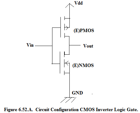
In the circuit given in Figure 6.52.A we find that body of (E)PMOS which is N-tub is connected to the source of PMOS which is P+.
Similarly body of (E)NMOS which is P-tub is connected to the source of NMOS which is N+.
Source to Bulk Voltage (Vsb) is kept zero in both cases so that Threshold voltage is maintained constant. If Vsb is not zero then Threshold Voltage will become a function of Vsb given by the following relation:

γ = body-effect parameter;________________________________________________
2φ F = surface potential parameter;___________________________________________
Since both MOSs are Enhancement type hence both are Normally OFF type therefore their channels are shown broken.
Notification Switch
Would you like to follow the 'Solid state physics and devices-the harbinger of third wave of civilization' conversation and receive update notifications?

|
|
|
|
|

|
|
|
|
|

|
|

|
|

|
|

|
|

|
|

|