

| << Chapter < Page | Chapter >> Page > |
Chapter 6_IC Fabrication Technology from 1960 todate_Part 2
6.5 Vertical NPN Transistor realization in IC Technolgy
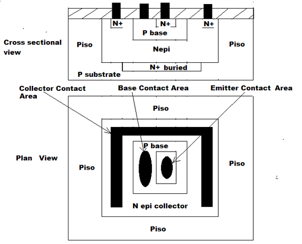
Figure 6.20 Stripe Geometry Vertical NPN Transistor in IC chip.
Section 6.6 Diode realization in IC Technology
Diode realization: A ‘n - p – n’ transistor is essentially a back to back diode. Hence any of the two junction diodes or both may be used for diode application. Therefore there are five possible combinations of e, b, c terminals by which diode can be achieved. But out of this c, b terminals shorted and used as anode whereas emitter terminal used as cathode gives a diode which has optimum performance parameters. The configuration is given in Fig.(6.21).
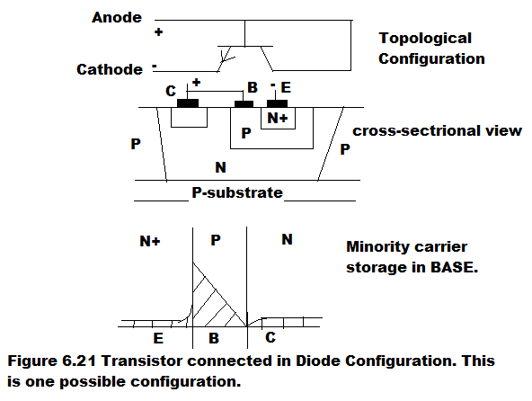
c-b shorted diode configuration of transistor has minimum storage delay or recovery delay time t d .
(t d = delay involved in switching a diode from ON to OFF conditions). t d is typically 9nsec. This diode is still a transistor in active region, since c-b is shorted hence it is still reverse biased. Diode isolation island is also provided with a buried layer so as to reduce series collector resistances. This enables the diode to give least forward bias voltage. Also this has the least leakage current flowing under reverse bias condition since the leakage current of E-B junction only comes into picture (E-B junction has smaller cross sectional area and has least depletion width and leakage current I O in reverse bias condition is predominantly the generation current in depletion width namely I g = q g X m A
g = generation rate,
X m = depletion width at the given reverse voltage,
A= cross sectional area of the junction.
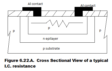
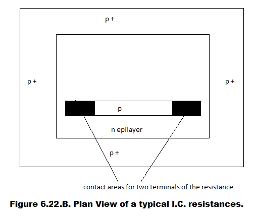
Section 6.7 Resistance realization in I.C. Technology:
p type diffusion for base gives a sheet resistance R sh = 200 ohms per square. By taking long strip like configuration of base diffusion, various resistances are realized. In Fig. (6.22) the resistance is given.
Section 6.8 Capacitor realization in IC Technology :
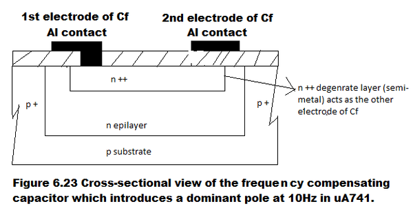
In uA 741 the frequency compensating capacitor C f = 30 pF is monolithically implemented. For I.C. realization of C f , silicon dioxide is used as the dielectric sandwiched between metallic Al layer and n+ degenerate layer. The n+ region is deposited during emitter diffusion step. The cross sectional view of the capacitor is given in Fig. (6.23)
“Introduction to Integrated circuits “ by Grinich and Jackson, the photomicrograph of uA 741 is given. As can be seen from the photomicrograph, 30 pF capacitor takes a significant chip area. Therefore it is neither economical nor practical to integrate circuits using capacitances.
Section 6.9 p-n-p transistor realization:
Here the n epilayer is used as the base and p diffusion for forming the base of n-p-n transistor is used for forming the collector and emitter of p-n-p transistor. The cross-sectional view of p-n-p transistor which is also known as lateral transistor is shown in Fig. (6.24). This is known as lateral transistor as the minority carriers flow laterally.
Notification Switch
Would you like to follow the 'Solid state physics and devices-the harbinger of third wave of civilization' conversation and receive update notifications?

|
|

|
|
|
|
|
|
|
|

|
|

|
|
|
|
|

|
|

|
|

|