

| << Chapter < Page | Chapter >> Page > |
SSPD_Chapter 6_Part 6_MOS IC Fabrication_concluded
6.6.5. Contact and Local Interconnect Formation.
A means of interconnecting the components on the wafer has to be found out and a means of bringing the input and output pads of the Silicon Chip to the external pins of the IC package has to be devised. At the present state of art of IC Technology, three levels of interconnections are provided. Lowest level is called Local Interconnects.
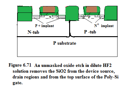
The first step in this direction is to remove the oxide from the contact pads of Source, Drain and Gate. No mask is required for this step. Just a short dip in HF acid removes the screen oxide, 10nm thick. This step is shown in Figure 6.71.
Next the whole wafer is covered with Titanium by sputtering as shown in Figure 6.72. The metal layer is shown n black. The thickness of Ti is 50 to 100nm. Sputtering is one of the Physical Vapour Depositon technique. In a sputtering system, the desired material (Ti in this case) are physically knocked off a solid target with Ar + ions. The Ti atoms are uniformly deposited. We will give the details of Physical Vapour Depositon in the next section.
Next the wafers are heated in N 2 ambient at 600 to 700°c for about 1 minute. There two kinds of reactions:
First is Ti + 2Si → TiSi 2 where Ti is in contact with Si or Poly-Si. Titanium Salicide (TiSi 2 ) is an excellent conductor and shown in navy blue in Figure 6.73. TiSi 2 forms the very low resistance contact pads to source, drain and gate.
Second is Ti + N→TiN where there is no contact with Si. . It is shown as light blue in Figure 6.73. TiN is also a conductor but not as good as metal hence used as ‘local’ interconnect. Long interconnects of TiN will cause unacceptable RC delays.


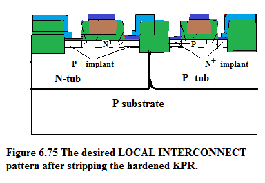
Mask 11 is used for etching out the local interconnect pattern as shown in Figure 6.74. Where SiN 2 is to be retained is protected by 200nm thick exposed KPR. Elsewhere KPR is removed by developer. Exposed KPR is annealed so as to become 100% resistant of the etchant. Next the wafer is dipped in Ammonium Hydroxide:Hydrogen Peroxide: Water solution in mass ratio of 1:1:5. This etchant etches away the exposed SiN. Thus we get the desired local interconnect pattern as shown in Figure 6.75. Hardened KPR is stripped away either by organic solvent or by O 2 plasma etching. After KPR stripping, we heat it in an inert ambient at 800°C for 1 minute. This reduces the sheet resistance of TiN and TiSi 2 to the final value of 10Ω/sq and 1Ω/sq.

6.6.6. Multilevel Metal Interconnect Formation- The Back-End Process.
After making the local interconnect we have to make the second level interconnect(metal level1) and third level interconnect (metal level2). For this we do confomal deposition of SiO 2 over the portion shown in Figure 6.76. This is done by CVD or LPCVD. This is thick layer of SiO 2 1 micron thick. This helps cover up the undulations on the local interconnect level. If these undulations or non-planar nature of the first level interconnect is not evened out then it is going to give rise to serious reliability problem in the subsequent interconnections. This thick layer of conformally deposited Oxide is doped with Phosphorous or with Phosphorous+Born combined resulting in PhosphoSilicate Glass(PSG) and BoroPhosphoSilicate(BPSG) respectively. In some cases an undoped SiO 2 layer is added on top of PSG or BPSG.
Notification Switch
Would you like to follow the 'Solid state physics and devices-the harbinger of third wave of civilization' conversation and receive update notifications?

|
|

|
|

|
|

|
|

|
|

|
|

|
|

|
|

|
|

|