

| << Chapter < Page | Chapter >> Page > |
SSPD_Chapter 6_Part 6_MOS Fabrication Technology_Concluded
Section 6.6.3 Gate Formation.
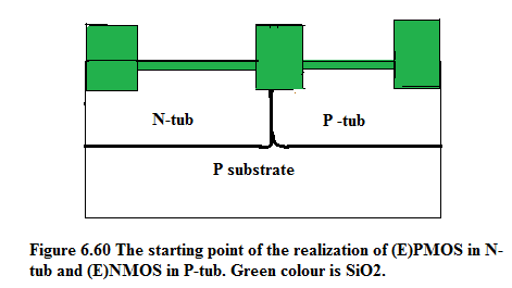
In the preceding section we saw how the twin tub is fabricated for realizing the complementary symmetry MOS also known as CMOS. If we choose the process option of P-implant below Field Oxide then the crss-sectional view is as shown in Figure 6.51. If we choose the process option of incorporating buried and epitaxial layer then the cross-section looks like Figure 6.59. For simplicity we will start with the twin tub as described in Figure 6.48. Now the critical part of MOS has to be fabricated namely P-channel and N-channel in normally-off PMOS and normally-off NMOS respectively. In other words we are fabricating (E)PMOS and (E)NMOS.
For the convenience of the reader Figure 6.48 is being reproduced here as Figure 6.60.
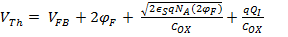
6.6.3.1. To precisely control the threshold voltage in the range 0.5 to 0.8 Volt, we do a second ion-implant of Arsenic or Phosphorous in N-tub and Boron in P-tub sequentially just below the gate oxide. The dose of this second ion-implant is calculated from Equation 6.22.
Q I = implant dose in atoms per cm 2 _________________________________________
Here V FB = flat band voltage = gate voltage required to compensate for the work function difference in the gate metal and semiconductor = φ M – φ S ;______________________
N A = doping density of P-tub which is going to host (E)NMOS before the critical ion-implant of Boron;_______________________________________________________
And ε S = permittivity of Silicon = absolute permittivity of free space × relative permittivity of Silicon;___________________________________________________
C OX = unit area capacitance of the gate oxide;

t OX = thickness of the gate oxide . This has to be precisely controlled inorder to achieve a precision in the threshold voltage.
Here it is assumed that implant dose is located near the Si-SiO2 interface inside the respective MOS depletion region.
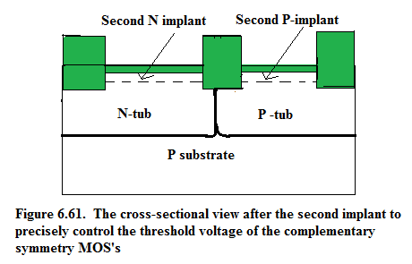
Mask 4 is used for selectively ion implant the P-tub with Boron at a dose implant of 1 to 5×10 12 /cm 2 at 50 to 75 keV. The energy is high enough to pass through the gate oxide but low enough to lie near the Si-SiO2 interface,
Mask 5 is used for selectively ion implant the N-tub with Arsenic or Phosphorous at a dose implant of 1 to 5×10 12 /cm 2 at 100 keV. The P-channel implant in N-Tub would be at a higher energy because Arsenic is heavier.
So the final cross-sectional view would be as shown as in Figure 6.61.
6.6.3.2. Regrowth of Gate Oxide to the precision required for the Threshold Voltage.
Gate area Silicon Dioxide layer has undergone two times battering under the two ion-implants hence the quality has deteriorated. Therefore it is important that it is stripped by dilute hydrofluoric acid and regrown to a precise thickness as demanded by the threshold voltage. Table 6.13 gives the typical gate oxide thickness for different generations of technology. After the gate-oxide is regrown to the precise thickness we go to the step of Poly-Si(heavily doped)Gate contacts. PolySi gate contacts were used before 45nm for achieving lower threshold voltage. But at 45nm technology, leakage current from the gate and the subthreshold current through the channel started deteriorating leading to increased thermal dissipation even in stand-by condition therefore thicker gate oxide thickness along with high – K dielectric such as Silicon Oxynitride was adopted as the gate dielectric. This reduced the standby dissipation but created the new problem of Fermi-pinning which led to the loss of control over the threshold voltage. Hence PolySi was replaced by Metal Contact. Thus at 45nm and below generation of technology, PolySi-SiO2 was replaced by MG-HK.
Notification Switch
Would you like to follow the 'Solid state physics and devices-the harbinger of third wave of civilization' conversation and receive update notifications?

|
|

|
|

|
|

|
|

|
|

|
|

|
|

|
|
|
|
|
|
|