

| << Chapter < Page | Chapter >> Page > |
The critical influence of temperatures on the diffusion profile has forced the semiconductor industry to acquire extremely sophisticated furnaces and controls, capable of holding temperatures in the range of 1000-1300 o C to a tolerance of + 0.5 o C in order that I.C ‘s can be manufactured reproducibly. A tolerance of + 0.5 o C enables one to achieve a tolerance of + 5 or + 10 percent in the diffusion depth which is critically linked to W(base width) a very important device parameter. A still closer tolerance in diffusion depth can be achieved by Ion Implantation.
6.4.8.3 Typical diffusion systems:
An impurity compound in its vapour form, sweeping across the wafers, is used as the corresponding impurity source. Impurity compound reacting with silicon releases the dopant which subsequently diffuses into the wafer. B 2 O 3 , BCl 3 and BBr 3 are used as sources of boron (p type dopant) and P 2 O 5 , POCl 3 are used as sources of phosphorous. In case of solid diffusion source such as P2O5 ,the solid impurity compound is heated in a chamber at a much lower temperature than that of wafers and a carrier gas such as oxygen is passed over the vaporizing P2O5, carrying it to the wafers.
2P 2 O 5 (gas)+5Si(solid)-→4P+5SiO 2 (solid).
Through the above chemical reaction , P is released and it diffuses into silicon . Simultaneously oxide layer is formed on wafer surface .A solid source is generally used for pre-deposition. B 2 O 3 is used for boron and As 2 O 3 for arsenic .
In case of liquid diffusion source , the carrier gas is bubbled though or passed over the liquid impurity compound which is kept in a flask heated to fixed temperature .The liquid vapour is carried by the carrier gas to the wafers where after chemical reaction , the dopant is released. The sources are POCl3 for phosphorous and BBr3 for boron deposition
A gaseous diffusion source may be used directly or diluted with some other gases.
A typical apparatus for P diffusion using POCl 3 is shown in Fig.(6.14).
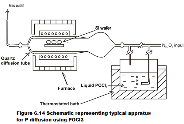
A carrier gas is bubbled through heated POCl 3 (the diffusion source). The impurity compound in vapour form reaches Si wafers and releases P atoms for diffusion. Typically the carrier gas is a mixture of N 2 and O 2 in the ratio of 3:1. This particular ratio leads to the formation of the moderate film of phosphorous –silicon glass necessary for surface protection and yet avoids excessive oxide formation which would otherwise create difficulty in photo resist processing. Practical device structures are limited to not more than three diffusion.
By several diffusion steps the total concentration of impurities below the surface become very large which reduces the electron and hole diffusion coefficients (and hence mobilities) by increasing the impurity scattering and reduces the carrier life time by introducing recombination centers in the crystalline structure. Also the total concentration under surface may reach the upper limit set by solubility so much so that further diffusion and compensation may not be possible. Hence sequential diffusions employed in formation of a device are limited to three.
Notification Switch
Would you like to follow the 'Solid state physics and devices-the harbinger of third wave of civilization' conversation and receive update notifications?

|
|

|
|

|
|

|
|

|
|

|
|
|
|
|

|
|

|
|
|
|