

| << Chapter < Page | Chapter >> Page > |
SSPD_Chapter 5_Section 5.3_Supplement_Photo-Diode_I-V curve.
The I-V Characteristics of a Photo-Diode is exactly the same as a classical diode except that there is an added family of curves due to illumination. Under reverse-bias, there is the DARK classical reverse leakage current which is of ‘nA’ magnitude. Under illumination condition, there is a family of curve under different illuminance condition as predicted by Equation 5.3.7 :

Using Equation 5.3.7. we generate a Table 5.3.2. for a photo-diode which has internal quantum efficiency = 0.9 and it is being excited by 1000nm IR light under different illuminance condition.
Table 5.3.2. Generation of Photo Current in reverse-biased Photo-Diode with internal quantum efficiency = 0.9 and irradiated by 1000nm IR light under different illuminance condition.
| P abs (μW) | I photo (μA) |
|---|---|
| 10 | 7.259 |
| 20 | 14.5 |
| 100 | 72.6 |
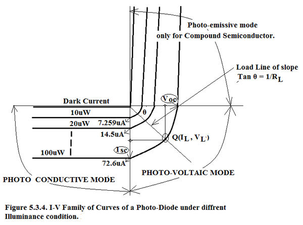
Assuming that we are using Ge-Photo Diode, the family of I-V curves under dark condition and under various illuminance condition is given in Figure 5.3.4. As seen in the Figure 5.3.4. IIIrd Quadrent is Photo-Conductive Mode, IVth Quadrent is Photo-Voltaic Mode and Ist Quadrent is Photo-Emissive Mode only for Compound Semi-Conductors.
In Photo-Conductive Mode, under reverse bias condition Photo-Diode conducts and acts as a Constant Current Source(CCS) to different extents according to the Illuminance condition. Under Dark Condition, CCS is open. With 10μW illuminance it acts as CCS of 7.259μA, with 20μW illuminance it acts as CCS of 14.5μA and with 100μW illuminance it acts as CCS of 72.59μA.
In fourth quadrent, Photo-Diode has no Bias Voltage. Under 100μW illuminance, the Y-intercept of the corresponding I-V curve gives the short-circuit current (I SC ) generated by the photo-cell and the X-intercept of the same curve gives the open-circuit voltage (V OC ) generated at the open circuit terminals of the photo-cell. When the Photo-Cell is terminated by load resistance R L then there is load line of slope=Tan θ = 1/R L. . This Load Line intersects the I-V curve of the photo cell at Q(I L ,VI L ). This Q-point tells us the current delivered to the terminated load. There is a particular Q-point on the I-V curve which maximizes the output power (I×V). A load matching circuit ensures that the cell operates at that point.
“Solar Energy is diffuse. Each square meter of solar cells can produce 25W of continuous power when averaged over day, night and sunny/cloudy days. The average electricity consumption of the world is over 10 12 W. If all he electricity is to be produced by solar cells, the cells need to cover a huge 200km by 200km area. Therefore low cost and high energy conversion efficiency, defined as the ratio of the electric output to the solar energy input, are important. Solar cells can be made of amorphous or polycrystalline as well as single-crystalline semiconductors. The first two types are less expensive but also less efficient in electricity generation”.[“Modern Semiconductor Devices for Integrated Circuits”, by Chenming Calvin Hu, Pearson 2010].
“The best solar cell efficiency(~24%) is obtained with E g values between 1.2eV and 1.9eV. Commercial rooftop silicon solar cell panels have conversion efficiencies between 15 to 29%. Tandem solar cells can achieve very high (over 30%) energy conversion efficiency by using two or more semiconductor materials. One with a large E g absorbs and converts the UV portion of the solar insolation to electricity and another of smaller E g material, positioned behind the first, does the same to the solar insolation that is not absorbed by the first material.”

FF is typically 0.75. The short-circuit current, I SC , is the photo-current given in Equation 5.3.7. and is directly proportional to the Illuminance condition.
Section 5.3.1. Application of Photo-Diode as demodulator in Optical Fiber Communication.
Optical Fiber Communication(OFC) is rapidly supplanting the copper wired Communication because of inherent advantage of OFC. OFC offers almost an infinite Band-Width hence large number of channels can be Frequency-Divison-Multiplexed (FDM) or Time-Divison-Multiplexed (TDM). Plus it is very light weight, much less voluminous and hence very cheap in handling. Its long haul, heavy traffic property makes it very attractive proposition in terms of cheaply affordable communication means by common masses. Therefore Photonics has assumed a very big importance both as detectors as well as photo sources.
So the most popular application of Photo-Diode is as Demodulator in OFC as shown in Figure 5.3.5.
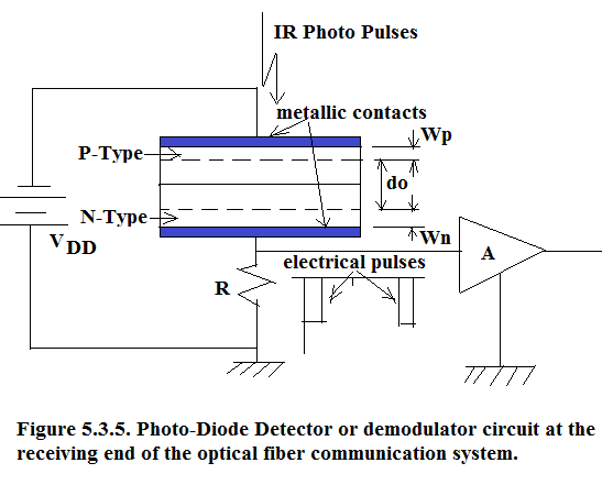
Photo-Pulses coming down the Optical Fiber Link are coupled into the photo-detector. In Photo-Diode, photo-pulses excite the photo-current pulses. These photo-current pulses, flowing through the resistance R of the detector circuit, produce voltage pulses. The voltage pulsesa are amplified by the Amplifier and passed on to Digital Signal Processing Chip.
Notification Switch
Would you like to follow the 'Solid state physics and devices-the harbinger of third wave of civilization' conversation and receive update notifications?

|
|

|
|

|
|

|
|

|
|

|
|

|
|

|
|

|
|

|