

| << Chapter < Page | Chapter >> Page > |
AE_Lecture 8_MOSFET&JFET_Part A continued.
In Part A of Lecture 8 we have seen the quantitative formulation of Enhancement and Depletion type MOSFET in Triode as well as in Pentode region. In this lecture, the continuation of Lecture 8_Part A, we will study the quantitative formulation of nJFET in ohmic and saturation region also known as triode and pentode region respectively.
Enhancement Type MOSFET was termed as Normally-Off device since with Gate-Voltage zero we have no current.
Similarly Depletion Type MOSFET is termed as Normally-On device since here even under Gate Voltage zero we do have a drain current because in NMOS(D), n-channel has been ion-implanted at fabrication stage hence it conducts at zero Gate Voltage.
In exactly the same fashion, JFET has a conducting channel at Gate Voltage zero. Hence it conducts under zero Gate Voltage therefore it is called Normally – On device. It is a depletion-mode device.
The physical structure of nJFET in a simplified manner is given in Figure 1.
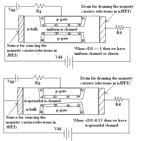
Figure 1. Physical structure of nJFET is given for negligible Drain-to-Source biasing and significant Drain-to-Source biasing respectively.
For negligible Drain-to-Source biasing, we have uniform n-channel as shown in the upper diagram. In this biasing condition, nJFET is operating in ohmic region or in Triode region.
For V DS >0.1 V, we have trapezoidal n-channelas shown in the lower diagram. The device is still in Triode region but its ohmic behavior is non-linear.
When V DS = (V GS – V P ) then the n-channel gets pinched off near the Drain and current saturates at that point. Now the device has entered saturation region. For V DS >(V GS – V P ), the current remains constant and device is said to be in Pentode region.
In Ohmic Region:
i D = K n [ 2(v GS – V P ) v DS – v DS 2 ] for 0<v DS ≤ ((v GS – V P )……………………….1
For small values of v DS ,
i D = K n [ 2(v GS – V P ) v DS ]……………………………………………………………2
At v DS * = (V GS – V P ), device enters the saturation region since channel is pinched off near the drain.
In saturation region, irrespective of v DS current becomes constant at the value decided by v DS * = (V GS – V P ). Substituting v DS * = (V GS – V P ) in Equation 1, we get:
I D = K n (V GS – V P ) 2 for v DS ≥ v DS * …………………………………………3
At V GS = 0, we have I D = K n ( -V P ) 2 = this denoted by I DSS ;
Hence

Typical values of Pinch-off voltage V P = 0 to -25V and typical values of I DSS is from 10µA to 10A.
For a given value of I D , Equation 3 gives two values of V GS . Only one value is physically tenable. It must lie in the range:
……………………………….V P <V GS <0
The line of demarcation or the pinch-off locus is a parabola. By substituting
v DS * = (V GS – V P ) in Equation 3 we get:
I D = K n (V GS – V P ) 2 = I D = K n (V DS * ) 2 which is a parabola and is defined as pinch off parabola.
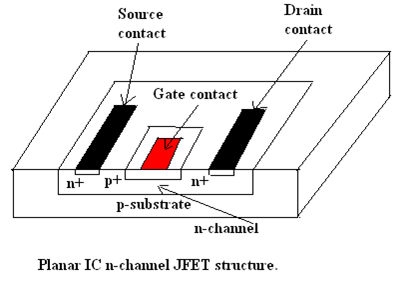
Figure 2. IC version of JFET.
Notification Switch
Would you like to follow the 'Solid state physics and devices-the harbinger of third wave of civilization' conversation and receive update notifications?

|
|

|
|

|
|

|
|
|
|
|

|
|

|
|

|
|

|
|

|