

| << Chapter < Page | Chapter >> Page > |
Section 4.3. Design Rules for fabricating BJT.
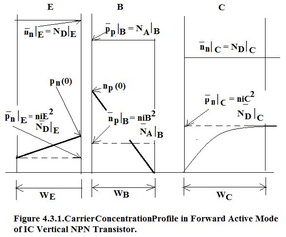
In Figure 4.3.1. the carrier concentration profile of Forward Active Mode BJT is revisited. Because of Forward Bias at EB Junction, electrons are injected from E to B and holes are injected from B to E.
In micro scale devices: base current had two parts= I B1 + I BB .
Therefore :


In nano- scale devices, I BB (the recombination current in Base) is negligible because of 10nm narrow Base. Hence the base current I B = Diffusion Current in Emitter = I Ep .
Therefore:

Let us define a quantity Gummel Number:

This is known as Emitter Gummel Number and it has the unusual dimension of sec/cm 4 .
At low level injection n n (z)= N DE in Emitter. Let n i 2 = n iE 2 and let D pE be constant throughout the Emitter Bulk then:
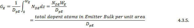
Eq.4.3.5. simplifies the Base Current Model and it contains all the subtleties of transistor design that affect I B :
By substituting Eq.4.3.5 in Eq.4.3.3. we get:

In exactly the same manner, collector current I C can be determined.


Defining Base Gummel Number as follows:

Taking the special case of low level injection p p (z)= N AB in Emitter , n i 2 = n iB 2 and D nB be constant throughout the Emitter Bulk we get:
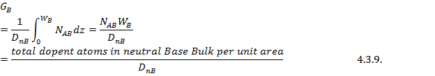
Therefore

Section 4.3.1. DC Current Gain of CE BJT .
Short Circuit CE BJT Current Gain = I C / I B = β F ________________________________4.3.11.
Using Eq.4.3.10 and Eq.4.3.6. we get :
Short Circuit CE BJT Current Gain= β F = G E /G B
Therefore
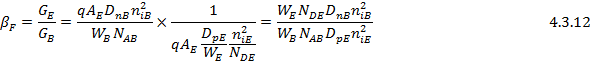
From Eq.4.3.12.in order to obtain large β F = 100, we must have high Emitter Doping and light Base Doping but light Base Doping will lead to large Base Spreading Resistance r x which leads to deleterious effect on high current and at high frequency operation. So we strike a balance by keeping Emitter doping at 10 20 /cc and Base Doping at 10 18 /cc .
To obtain high Emitter Injection Efficiency γ we must examine the expression γ.
Injection Efficiency had been defined as:
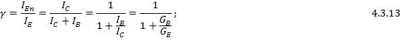
If β F = 100 then α F = 0.99.
Since α F = I C /I E = β F / (1+ β F ) and β F = α F /(1- α F )
Injection Efficiency = γ = 1/(1+1/ β F ) = α F ;
Section 4.3.2. Emitter Band Gap Narrowing.
Because of heavy doping effect there is a Band Gap Narrowing by ∆V. This results in a reduction of Short Circuit CE BJT Current Gain.
We know that :

If there is Band Gap narrowing by ∆V then Eq.4.3.14 gets modified to:

Dividing Eq.4.3.15 by Eq.4.3.14 we get :

Substituting Eq.4.3.16 in Eq.4.3.12 we get:
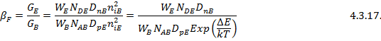
Typically ∆E = 0, 50meV, 95meV at less than 10 18 /cc , 10 19 /cc , 10 20 /cc , respectively.
Thermal energy is 25meV. Therefore at 10 19 /cc , 10 20 /cc , β F will fall by 1/7.39 and 1/36.6 respectively.
Section 4.3.3. Base Transit time and Charge Storage in Base.
Referring to Figure 4.3.1. the charge stored in the Base:

And Collector Current is:

We define Q FB /I C = Forward Transit Time = τ FB .
Dividing Eq.4.3.18 by Eq.4.3.19 we get:

We purposely make Base doping density linearly graded. This gives rise a built-in electric field which opposes Majority Carriers but support the diffusion of Minority Carriers from higher to lighter density. This electric field shortens the Transit Time in forward direction. Hence :

Therefore we get a better performance than expected. Therefore linearly graded base Transistors are referred to as Drift Transistor.
Typically Effective Base Width is 70nm and D nB = 10 cm 2 /s. This gives a transit time by Eq.4.3.20 as 2.5ps.
Therefore Transit angular frequency = ω T = 1/2.5ps = 400Grad/s
Transit Frequency = 400/(2π)=64GHz.
To date we have achieved 500GHz with Base Width of 10nm.
Notification Switch
Would you like to follow the 'Solid state physics and devices-the harbinger of third wave of civilization' conversation and receive update notifications?

|
|

|
|

|
|

|
|

|
|

|
|

|
|

|
|

|
|
|