

| << Chapter < Page | Chapter >> Page > |
AnalogElectronics_Lecture4_PartA_dc,low&high frequency model of CB BJT.
The DC model of BJT.
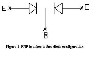
PNP is a face to face diode.
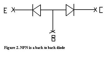
NPN is a back to back diode.
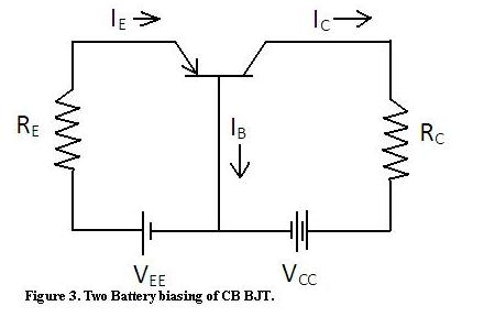
DC Biasing of CB BJT (Common Base BJT) In the figure base is grounded.
The DC model of CB BJT is called Eber Moll Model. It is a large signal model.
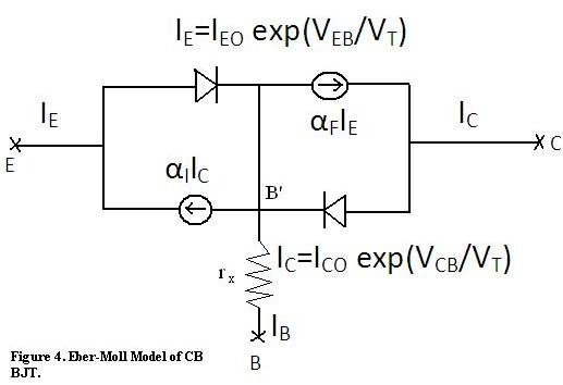
Figure 4. Eber Moll Model of PNP Transistor under no bias.
As can be seen from the Eber Moll Model:
α F I E is the controlled current source controlled by the current injected from E to B where α F is short circuit forward current transfer ratio.
α I I C is the controlled current source controlled by the current injected from C to B where α I is short circuit inverse current transfer ratio.
Because of asymmetrical doping density, [Heavy Emitter doping(10 19 /cc), Intermediate Base doping(10 17 /cc) and light Collector doping(10 16 /cc)]
emitter to base injection efficiency is 99%
whereas collector to base injection efficiency is less than 10% therefore (α I = 0.1)<<(α F =0.99).
Under Forward Active Mode :
EB diode is forward biased and CB diode is reversed biased. Hence current is being injected from emitter to base but no current is being injected from collector to base. Therefore EB diode is shown and CB diode has been omitted but there is reverse saturation current/reverse leakage current I CBO flowing through reverse biased CB junction. In fact there are two currents flowing across the CB junction. One is the leakage current I CBO and the other is the useful transistor current α F I E due to transistor action at EB junction.
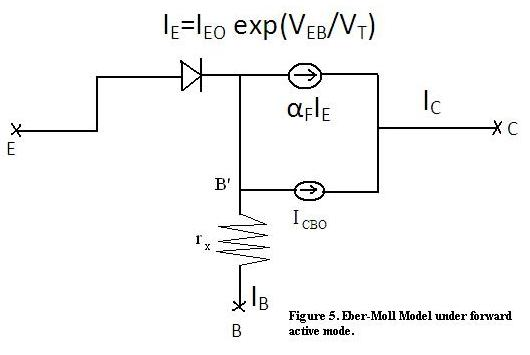
Figure 5. Eber Moll Model under Forward Active Mode.
LOW FREQUENCY MODEL OF CB BJT.
A capacitively coupled CB Amplifier is shown in Figure 6. It amplifies sinusoidal signal but blocks dc signal.
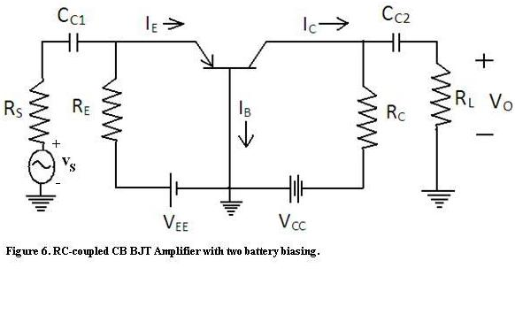
In Figure 6 we have capacitively coupled source and capacitively coupled load in CB BJT.
In Figure 6 we show a CB BJT Amplifier. Because of near unilaterality of CB BJT (h rb negligible), it is very suitable for RF tuned amplifiers. RF tuned amplifiers have a serious problem of parasitic oscillation because of output - input interaction and this interaction is due to h r (reverse transmission factor).
CE BJT has h re = 10 -4 hence CE BJT Amplifier is very prone to parasitic oscillations. But CB BJT has h rb = 10 -5 hence CB BJT is the configuration of choice for implementing RF tuned amplifiers.
Also capacitive coupling is used because once a Quiescent Point or DC operating point is set up we do not want it to be disturbed by load or source. That is load and source must be a.c. coupled but d.c. decoupled. Capacitive coupling serves this end.
Capacitively coupled Amplifiers (CE, CB&CC) are always ac amplifiers. But inverting amplifiers made of Op Amp with dual power supply is a direct coupled amplifier. There are no coupling capacitors. Hence they are dc amplifiers. DC amplifiers can amplify from dc to high frequencies.
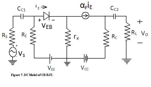
In Figure 7 we have the instantaneous model of CB Amplifier with signal coupled to it.
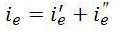
Therefore i E (instantaneous emitter current) = I E (emitter quiescent current) + i e (emitter incremental current);
Similarly we have i C = I C + i c and i B = I B +i b ;
Also I C = β F ×I B and i c = β f ×i b ;
Here β F = dc short circuit current gain and β f = incremental short circuit current gain.
In BJT : β F = β f ;
The instantaneous model also contains r x = r bb’ = base spreading resistance.
This is an ohmic resistance offered by the thin layer of P type silicon sand-witched between Emitter layer and Collector layer as shown in the cross sectional view of IC vertical npn BJT (Figure 8)
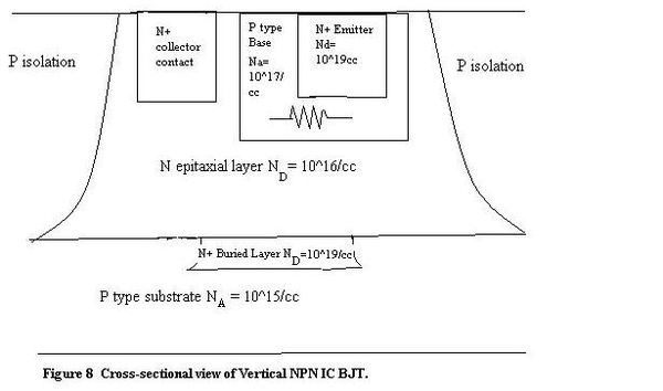
Figure 8. Cross sectional View of Integrated Circuit Vertical NPN BJT.
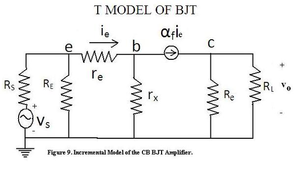
Figure 9. Incremental Model of CB BJT Amplifier.(the controlled current source is α f i e ).
This incremental model is known as the T-model of CB BJT.
As in incremental diode circuit, here also we short the DC Voltage Sources(V CC and V EE ), we open circuit DC Current sources such as (I CBO + α F I E ) but we retain the incremental current source α f i e .
The coupling capacitances are shorted.
EB Diode is replaced by incremental resistance r e =(V T /I EQ ).
The ohmic resistances are retained as they offer resistance to DC as well as incremental component of the current.
HIGH FREQUENCY MODEL OF COMMON BASE BJT
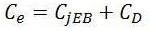
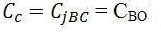
Under high frequency condition the Junction Capacitances associated with the depletion layers EB and BC and Diffusion Capacitance associated with minority carriers stored in base region start effecting the performance of the BJT. These parasitic capacitances effect the Frequency Response as well as the short circuit current gain.
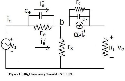
Figure 10. Incremental T-Model of the CB Amplifier Circuit at high frequency. (the controlled current source is α f i e )
At high frequency diffusion and junction capacitances come into play.
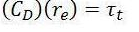
C D = more than 70pF.
Where

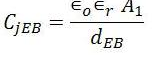
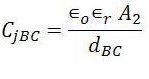


Here


α fo =short circuit incremental forward current transfer ratio at low frequency.
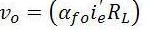
This is true only when we consider r c = infinity and C C to be open.
This means this model is valid only till


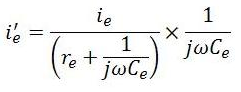
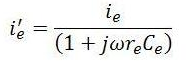
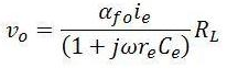
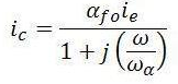
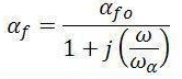
Here α f = short circuit current transfer ratio at all frequencies for CB BJT.
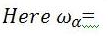
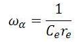
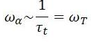
Here


The Bode Plot of the above expression of

Notification Switch
Would you like to follow the 'Solid state physics and devices-the harbinger of third wave of civilization' conversation and receive update notifications?

|
|

|
|

|
|

|
|

|
|

|
|

|
|

|
|

|
|

|