

| << Chapter < Page | Chapter >> Page > |
Analog Electronics Lecture 2_PartC_I-V output characteristics of BJT
Key words;BJT;
Abstract: This describes the D.C. parameters of BJT.
BJT Common Base Configuration :
For CB Configuration :
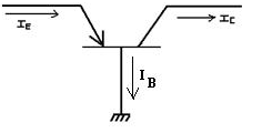
I C = α F MI E + I CBO
Where α F = D.C. Forward current transfer Ratio of CB BJT = I C /I E ;
M = Avalanche Multiplication Factor at Base-Collector Junction given by = 1/[1-(Vcb/BVcbo)^n]

Where n= Miller Indices =2~6
I CBO = Reverse leakage current at CB Jn with emitter open.
OUTPUT CHARACTERISTICS OF Common Base Bipolar Junction transistor
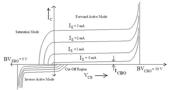
I C = I CBO when I E = 0 mA. This is the reverse leakage current at CB Junction with Emitter open and is of nA range.
BJT Common Emitter(CE) Configuration:
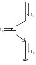
For CE Configuration :
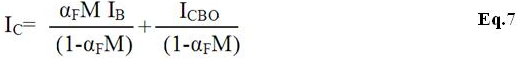
I C = α F MI E + I CBO
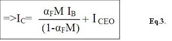
=>I C = α F M(I B +I C ) + I CBO
=>I C (1-α F M)= α F MI B + I CBO
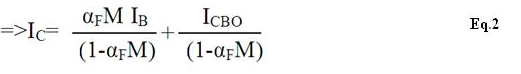
If M=1,
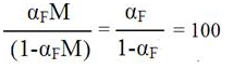
Where α F =0.99.
At low voltages we have M=1.
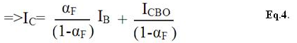
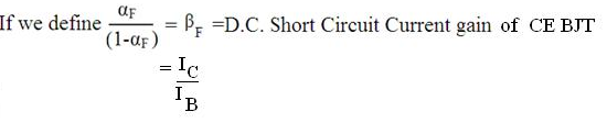
Then we get:
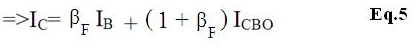
That is:

OUTPUT CHARACTERISTICS OF Common Emitter Bipolar Junction transistor
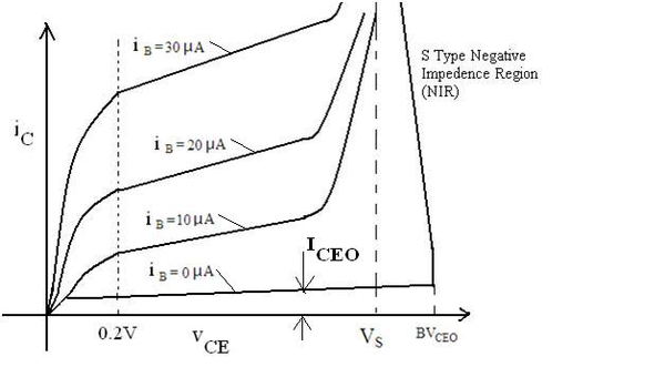
NOTE:-The slope in the figure is due to base width modulation which is also known as Early Effect.
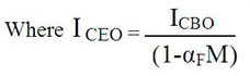
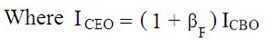
I C = I CEO when I B = 0 mA. This is the collector junction leakage current at CB Junction with Base open and is of µA range.
Let us consider :
If α F M =1, then
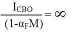
At this point , break over occurs. And we have BV CEO =Break-over Voltage with Base Circuit open.
When α F M =1
That is
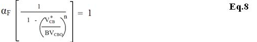
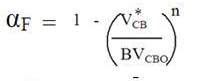
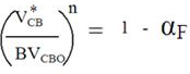
But :
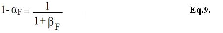
Thus :
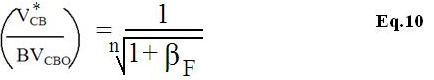
Thus:
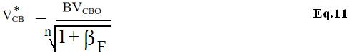
Putting the required Values i.e. BV CBO =30V, β F = 100 , we get V CB * =18 V = BVceo ;
Now we have to know more about BV CES (Breakover Voltage when the base circuit is shorted)
BV CBO >BV CEX >BV CES >BV CEO
Where BV CBO = Breakover Voltage of the collector base junction when the emitter circuit is open.
BV CEX = Breakover Voltage of CE BJT for a given termination R X at the base
BV CEO = Breakover Voltage of CE BJT when the base circuit is open.
BV CES = Breakover Voltage of CE BJT when the base circuit is shorted to ground.
BV CEX = Breakover Voltage when the base circuit is connected to ground through a source Resistance (R S ) .
By proper base termination, the permissible region of operation can be extended upto BV CBO .
Thus we have seen that breakover occurs at α F M =1. At low current α F is very small, almost about 0.1.Therefore voltage has to be taken to a large value to satisfy α F M =1. But as soon as breakover occurs large current starts flowing. With large current α F improves from 0.1 to 0.99. Hence α F M =1 is satisfied at lower voltage Vs. Therefore breakover curves settles down at Vs. This voltage V S is known as sustaining voltage. Because of the fact that :
V S <BV CEO
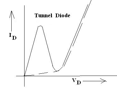
We get a S Type Negative Impedance Region(NIR). In SCR and UJT also we get S Type NIR but in Tunnel Diode as shown in the Figure below we get N Type NIR.
COMPARISON BETWEEN COMMON BASE AND COMMON EMITTER CONFIGURATIONS
| S.No. | COMMON BASE | COMMON EMITTER |
| 1 | h rb (reverse transmission factor)~10 -5 Thus it behaves as a near unilateral device. | h re ~10 -4 Thus it behaves as a non-unilateral device. |
| 2 | In RF applications the circuit has a high probability of parasitic oscillations but in CB because of near unilaterality , probability of parasitic oscillation goes down. Hence for RF applications CB is the preferred circuit configuration. | At low frequencies there is no danger of parasitic oscillations hence CE can be used even with poor reverse transmission factor. |
| 3 | h ob = 1/(2M)Thus it behaves as a near ideal current source. Thus it is very suitable for charging a capacitance with a constant current to generate a saw-tooth waveform. | h oe =1/(40K)Thus it behaves as a non-ideal current source. |
Both CB and CE are Current Controlled Current Source. CB is a near ideal CCCS whereas CE is a non-ideal CCCS.
Notification Switch
Would you like to follow the 'Solid state physics and devices-the harbinger of third wave of civilization' conversation and receive update notifications?

|
|

|
|

|
|

|
|
|
|
|

|
|

|
|

|
|

|
|

|