

| << Chapter < Page | Chapter >> Page > |
Chapter 4_Section 4.4_Design Rules for nJFET.
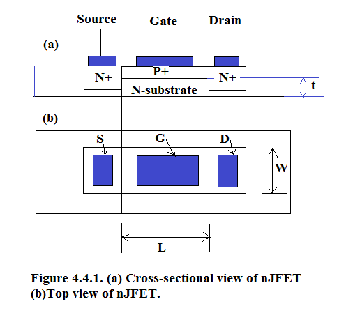
We have already discussed the structure and physics of nJFET in m38382.
We saw that in Triode Region (Ohmic Region):

V P = Pinch – Off voltage of the channel given by the following expression:

For small drain-source voltages (v DS <0.1V):

Therefore N-type Channel of nJFET offer linear resistance given by the following expression:

Thus at small voltages Gate Controlled linear resistances can be realized using a JFET.
In Pentode Region, the drain current saturates at V DS * = (V GS - V P ) :

At V GS = 0, i DS = I DSS and from Equation 4.4.5:

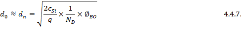
Here d n = depletion penetration in N-substrate at zero gate voltage and is given by the following expression:
The customer will specify the pinch-off voltage and I DSS . In practice these can range from
0 to -25V for Pinch-Off voltage and I DSS = 10μA to 10A.
From these specifications the fabrication parameters and geometrical dimensions can be determined.
Section 4.4.1.Design nJFET for pinch-off Voltage -1V and -2V.
Keep the Gate P+ doping at 10 19 /cc. Keep L=10μm and W=10μm.
Calculate the total thickness ‘t’ for pinch-off voltage at -1V and -2V. Also calculate the penetration of depletion width in the channel at Gate Voltage = 0V. This Data will be required while calculating I DSS .
Design procedure for V P = -2V.
Using Eq.4.4.2. for N D = 10 13 /cc we get t = 18.4μm and using Equation 4.4.7 we get d 0 =9.47μm.
At N D = 10 13 /cc the resistivity of the channel is 430.45Ω-cm. Using Equation 4.4.6. we get :
I DSS = 12.45μA.
If instead of N D = 10 13 /cc , N D = 10 14 /cc is used then we get t = 5.9μm and using Equation 4.4.7 we get d 0 =3 μm.
At N D = 10 14 /cc the resistivity of the channel is 43.45Ω-cm. Using Equation 4.4.6. we get :
I DSS = 40μA.
Design procedure for V P = -1V.
Using Eq.4.4.2. for N D = 10 13 /cc we get t = 14.6μm and using Equation 4.4.7 we get d 0 =9.47μm.
At N D = 10 13 /cc the resistivity of the channel is 430.45Ω-cm. Using Equation 4.4.6. we get :
I DSS = 3.47μA.
If instead of N D = 10 13 /cc , N D = 10 14 /cc is used then we get t = 4.7μm and using Equation 4.4.7 we get d 0 =3 μm.
At N D = 10 14 /cc the resistivity of the channel is 43.45Ω-cm. Using Equation 4.4.6. we get :
I DSS = 12μA.
Notification Switch
Would you like to follow the 'Solid state physics and devices-the harbinger of third wave of civilization' conversation and receive update notifications?

|
|

|
|

|
|

|
|

|
|
|
|
|

|
|

|
|
|
|
|

|