

| << Chapter < Page | Chapter >> Page > |
AE_Lecture8_Incremental Model of FET.
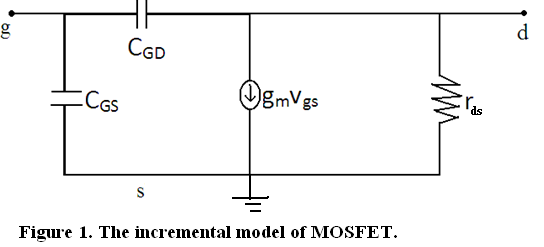
FET behaves as Voltage Controlled Current Source. Hence its model is as given in Figure 1.
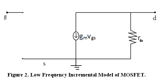
At low frequencies Capacitances can be considered to be open circuit. And the Incremental Model at low Frequencies will have infinite impedance as shown in Figure 2.
At low frequencies, input current is zero and short circuit current gain is INFINITY. But at high frequencies gate to source Capacitance due to overlap Capacitance ( overlap between source and gate) and Gate Oxide Capacitance and gate to drain Capacitance again due to overlap Capacitance ( overlap between drain and gate) and Gate Oxide Capacitance draw considerable currents. Hence Short Circuit Current Gain is finite and falls at the rate of 20dB/decade.
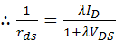
In the low frequency model, we have transconductance (g m ) and output impedance of the current source (r ds ).
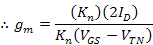
Derivation of Transconductance.


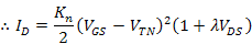
Due to channel length modulation the family of curves are not horizontal but have a finite slope.as shown in Figure 3. To account for this ,channel-length modulation parameter λ is introduced.
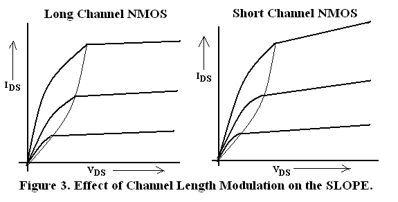
In long channel NMOS(with channel length of 10µm) of bygone MSI(Medium Scale Integration) and LSI(Large Scale Integration) era, the slope was minimal. But as packing density increased to 40 million transistors, lateral scaling reduced the channel length to 100nm. In short channel NMOS channel length modulation is very pronounced as seen in Figure 3.
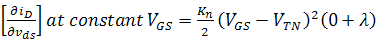
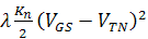
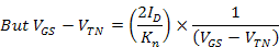
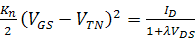
We know that

Amlification Factor=µ= g m ×r 0 = the maximum gain which can be achieved from a Common Source or Common Emitter Amplifier.
Combining Eq 1 and Eq 2 we get the following:
Amplification Factor of CS MOS Amplifier=[

Amplification Factor of CE BJT Amplifier=[

V A is the Early Voltage which was discussed in Lecture 3 in connection with the Static Output characteristics of CE BJT.
As seen above the amplification factor of CE BJT is independent of Quiescent Collector Current. From the Table we see that it is only 3400. But my research on CE BJT is showing that a much larger gain can be realized.
In the following Table we make a comparative study of BJT and FET.
| FET | BJT |
| Geometry dependent parameters
|
Geometry independent parameters |
| µ(amplification factor varies inversely with I D ) | µ(amplification factor is independent of I D ) |
| V
DS =10V,K
n =1
|
β o =100,V A =75V,V CE =10V |
| gm=
|
gm=
|
| Small signal approximation holds good for values:
|
Small signal approximation holds good for values:
|
| Much higher packing density because no isolation diffusion required. | Here isolation diffusion is required hence historically it is one generation behind as far as packing density is concerned |
| This is slower. The best clocking speed is 3GHz | BJT is historically much faster . The state of art in BJT is achieving 300GHz transit frequency. |
| Noise Figure is much better. This has no SHOT noise , no PARTITION noise. It has flicker noise. For Low Noise Amplifier cryogenically cooled MESFET. | Noise Figure is poorer because of SHOT noise, PARTITION noise and THERMAL noise. |
| I D (µA) | g m (×10 -3 S) | r ds (MΩ) | µ | I C (µA) | g m (×10 -3 S) | r π (kΩ) | r 0 (MΩ) | µ |
| 1 | 0.0476 | 85.2 | 4060 | 1 | 0.04 | 2500 | 85 | 3400 |
| 10 | 0.151 | 8.52 | 1280 | 10 | 0.4 | 250 | 8.5 | 3400 |
| 100 | 0.476 | 0.852 | 406 | 100 | 4 | 25 | 0.85 | 3400 |
| 1000 | 1.51 | 0.085 | 128 | 1000 | 40 | 2.5 | 0.085 | 3400 |
| 10,000 | 4.76 | 0.0085 | 40 | 10,000 | 400 | 0.25 | 0.0085 | 3400 |
HIGH FREQUENCY MODEL OF FET
In Figure 4, high frequency model of MOSFET is set up for calculating the short circuit current. We follow the same procedure as we followed in CE BJT.
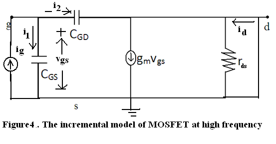
There are various values for C gs and C gd in Triode Region, in Pentode Region and in Cut-off Region. In Analog Electronics for linear applications we are concerned only with Pentode Region. So we will consider the two capacitances in Pentode or in Saturation Region.
C GS = (2/3) C GC + C GSO .W
C GD = C GDO .W
Where C GC = C OX .WL and C OX = (ε 0 . ε oxide )/D oxide F/cm 2 ;
C GSO = overlap capacitance between Gate and Source;
C GDO = overlap capacitance between Gate and Drain;
Since r ds is shorted therefore :
I 2 (jω) + I d (jω) = g m . V gs (jω) 3
V gs (jω) = I g (jω)/(jω(C GS + C GD ) 4
From Eq3 and Eq4:
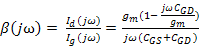
Eq 5 can be rewritten as :
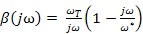
Where ω T = g m /( C GS + C GD ) = Unity Gain BW or Gain×BW or Gain BW Product(GBP);
And ω* = g m /C GD and β(jω) falls at 20dB per decade.
Through proper substitutions in GBP expression we get :
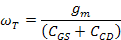
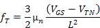
A reduction in channel length by a factor of 10 increases f T by 100.
In BJT GBP<1/(r x C µ )
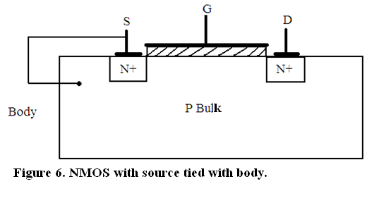
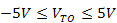
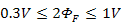
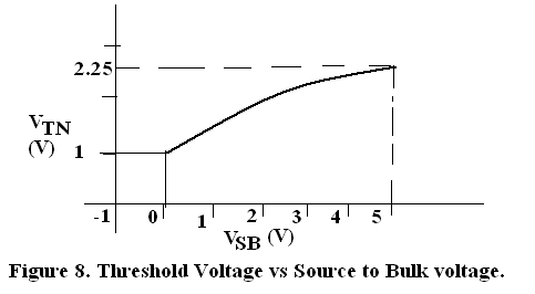
BODY EFFECT or SUBSTRATE SENSITIVITY
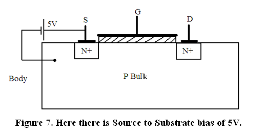
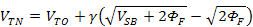
Where


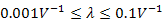
Typical Values are :-


Notification Switch
Would you like to follow the 'Solid state physics and devices-the harbinger of third wave of civilization' conversation and receive update notifications?

|
|

|
|

|
|

|
|

|
|
|
|
|

|
|
|
|
|

|
|

|