

| << Chapter < Page | Chapter >> Page > |
In Section 3.2.2. we have derived the Shockley Equation or the Ideal Diode Equation from the first principles of the forward biased diode. In the present section the same Ideal Diode Equation will be verified by studying the reverse biased diode. This analysis will give the physical origin of the reverse leakage current or the reverse saturation current. In Figure 3.11. the space charge region, the electric field and the potential gradient in a reverse biased diode is given.
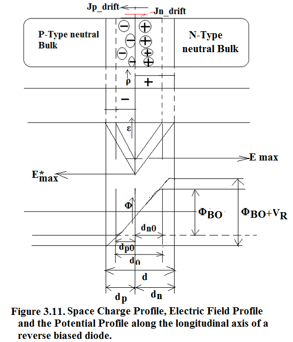
Under reverse bias, as seen from Figure 3.11., the depletion region widens, maximum Electric Field at the junction becomes more intense and built-in barrier potential is now (Φ BO +V R ).
Equation 3.2.9. gets modified to the following form:
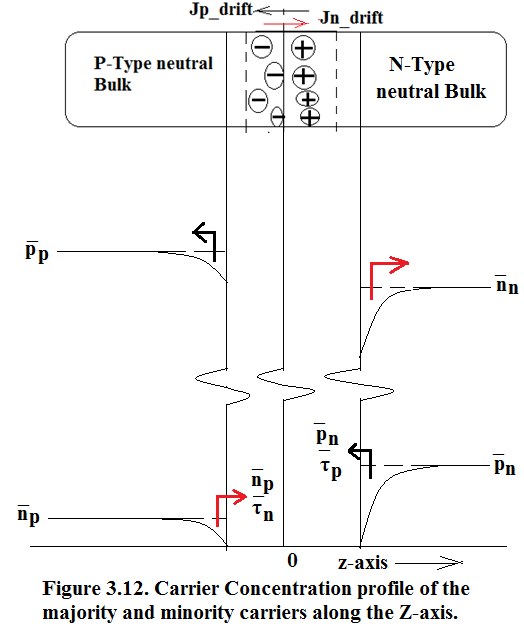
Diffusion current of majority carriers is completely stopped because of large barrier potential. There is only drift of the minority carriers in the reverse direction.By examining Figure 3.12 we can analytically deduce the drift currents and hence the total reverse leakage current. In Figure 3.12. the carrier concentration of a reverse biased diode is shown.
By Boltzmann relation,at the edge of the depletion region, minority carrier concentration is perturbed in the following manner:

Equation (3.2.4.2) tells us that under forward bias there is excess of carriers at the edge of the depletion region hence there is recombination and under reverse bias there is deficit of carriers and hence there is thermal generation of EHP and the the minority carrier is suppressed to zero at the edge of the depletion region hence the generation rate is:


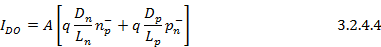
All the generated carriers within L n (diffusion length of electrons) manage to survive and reach the edge of the depletion region on the P-Side. Similarly All the generated carriers within L p (diffusion length of holes) manage to survive and reach the edge of the depletion region on the N-Side.Hence total reverse saturation current or reverse leakage current is as follows:
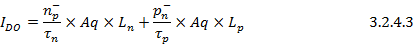
This is the same as the reverse leakage current in Equation (3.2.2.6).
The reverse leakage current in Equation (3.2.2.6) is:


Hence the Equations (3.2.4.3) and (3.2.4.4) are equivalent and they are due to the limited minority carriers being generated at the two sides of the depletion region. As soon as they are generated they drift down the potential gradient of the built-in barrier potential.
Since they depend upon the generation of the minority carriers hence they are very temperature sensitive and they double for every 10°C rise in temperature for Si as well as for Ge diodes.
3.2.4.1.Temperature dependence of I DO (reverse leakage current).
Rewriting Equation(3.2.4.4):
Therefore:

From Equation (3.2.4.5), it is evident that for small increments if we assume mobility and diffusion coefficient to be independent of temperature then I DO varies directly as n i 2 .
Notification Switch
Would you like to follow the 'Solid state physics and devices-the harbinger of third wave of civilization' conversation and receive update notifications?

|
|

|
|

|
|

|
|

|
|

|
|

|
|

|
|

|
|

|